Downloaded 83 times
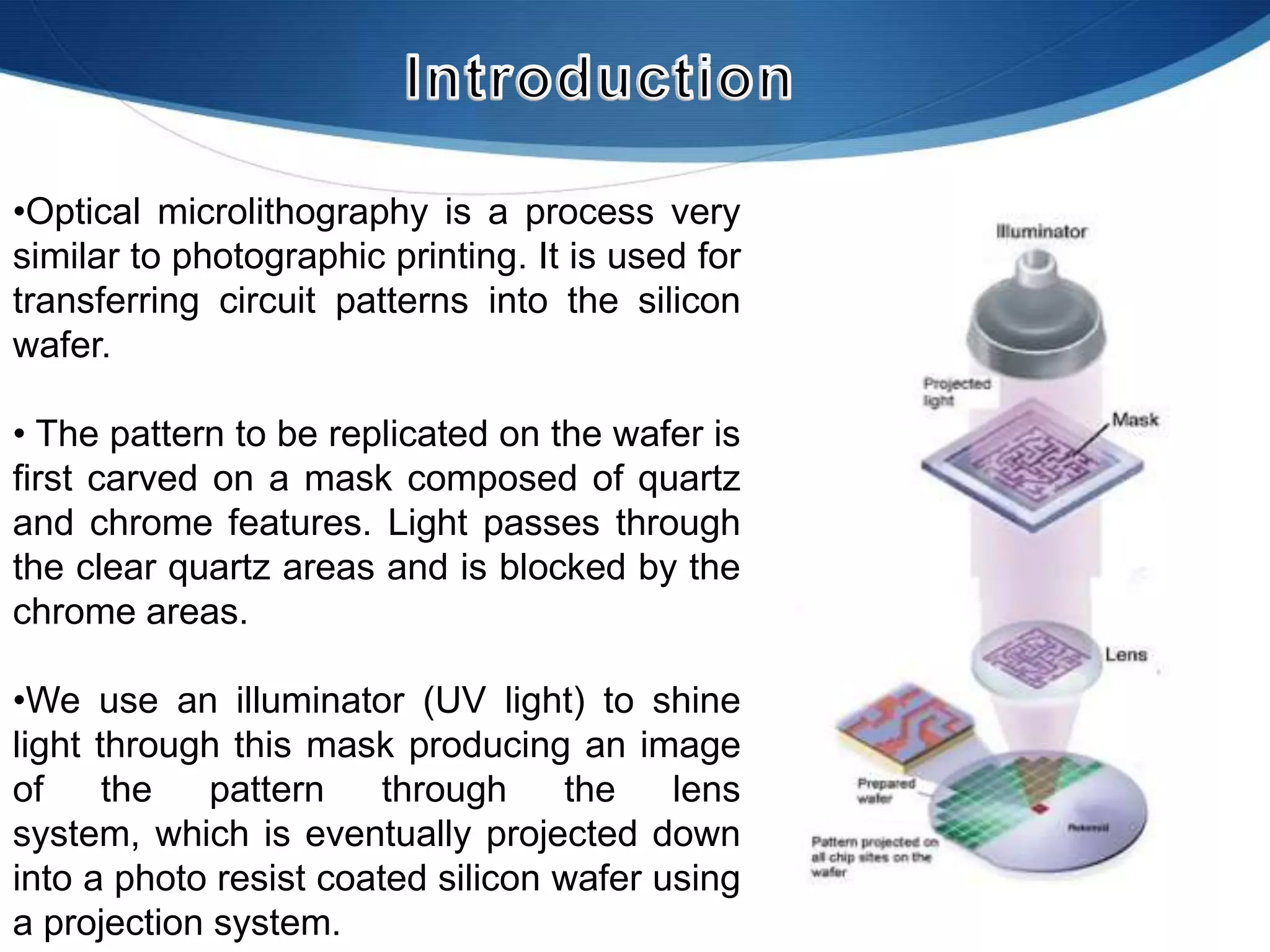
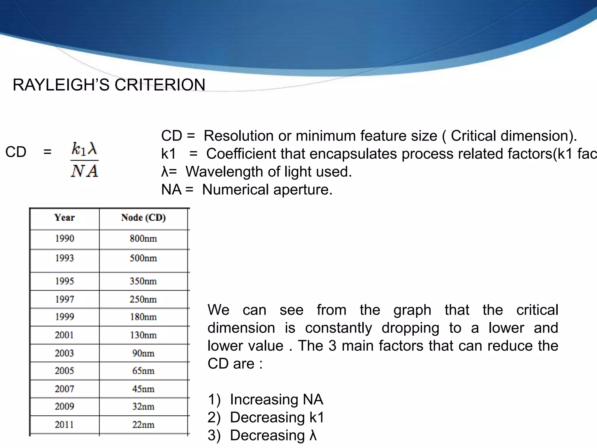
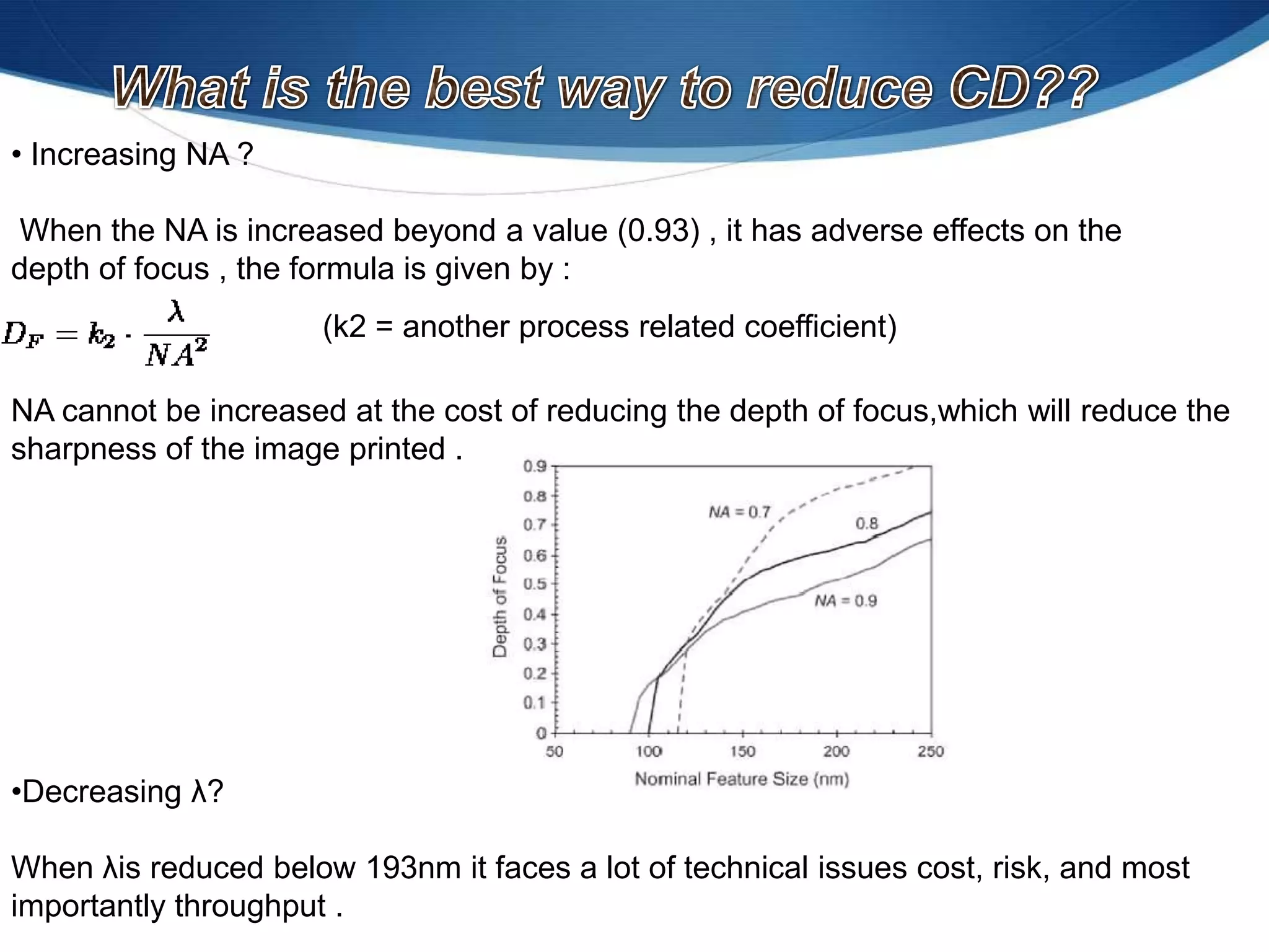
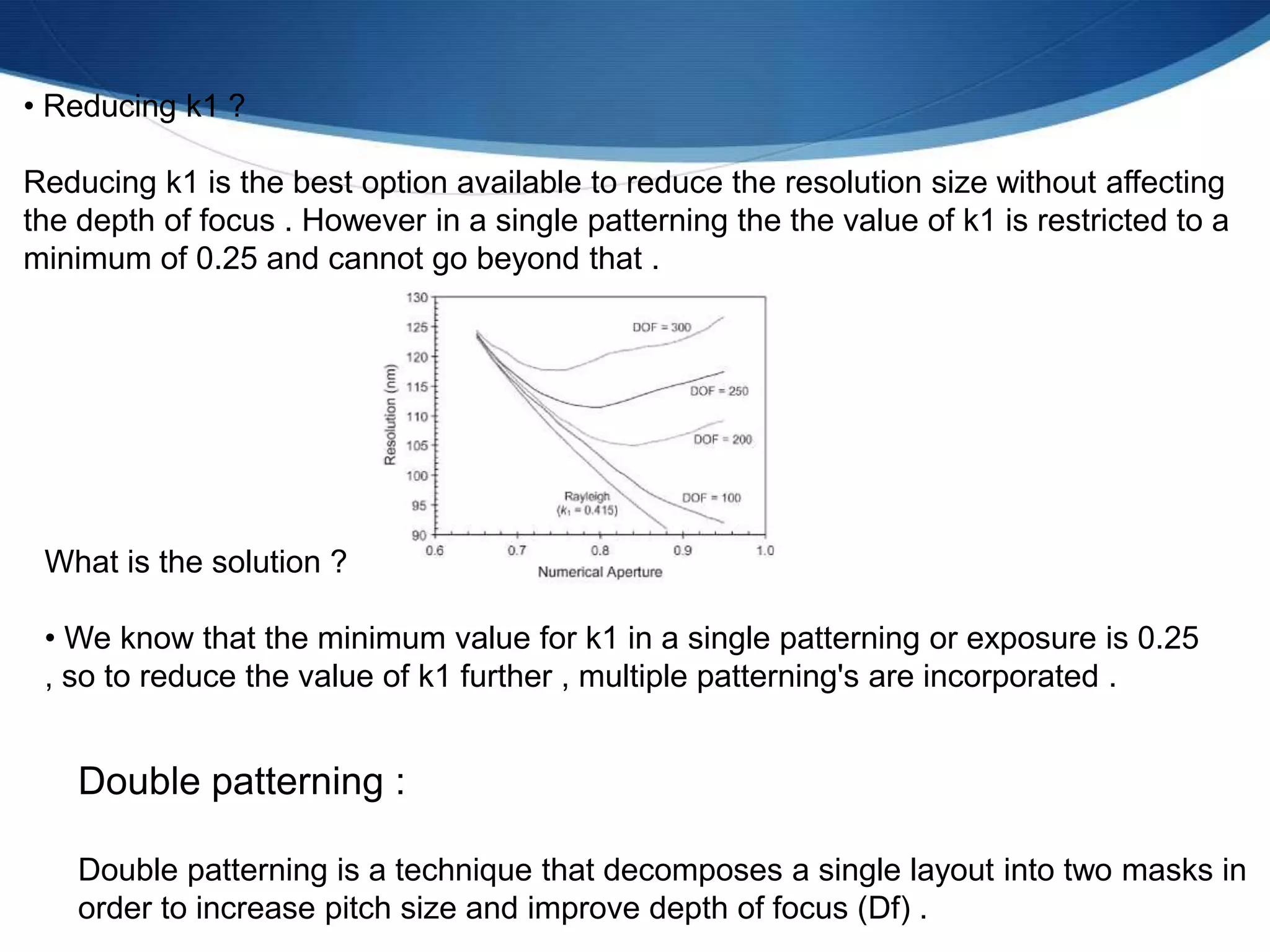
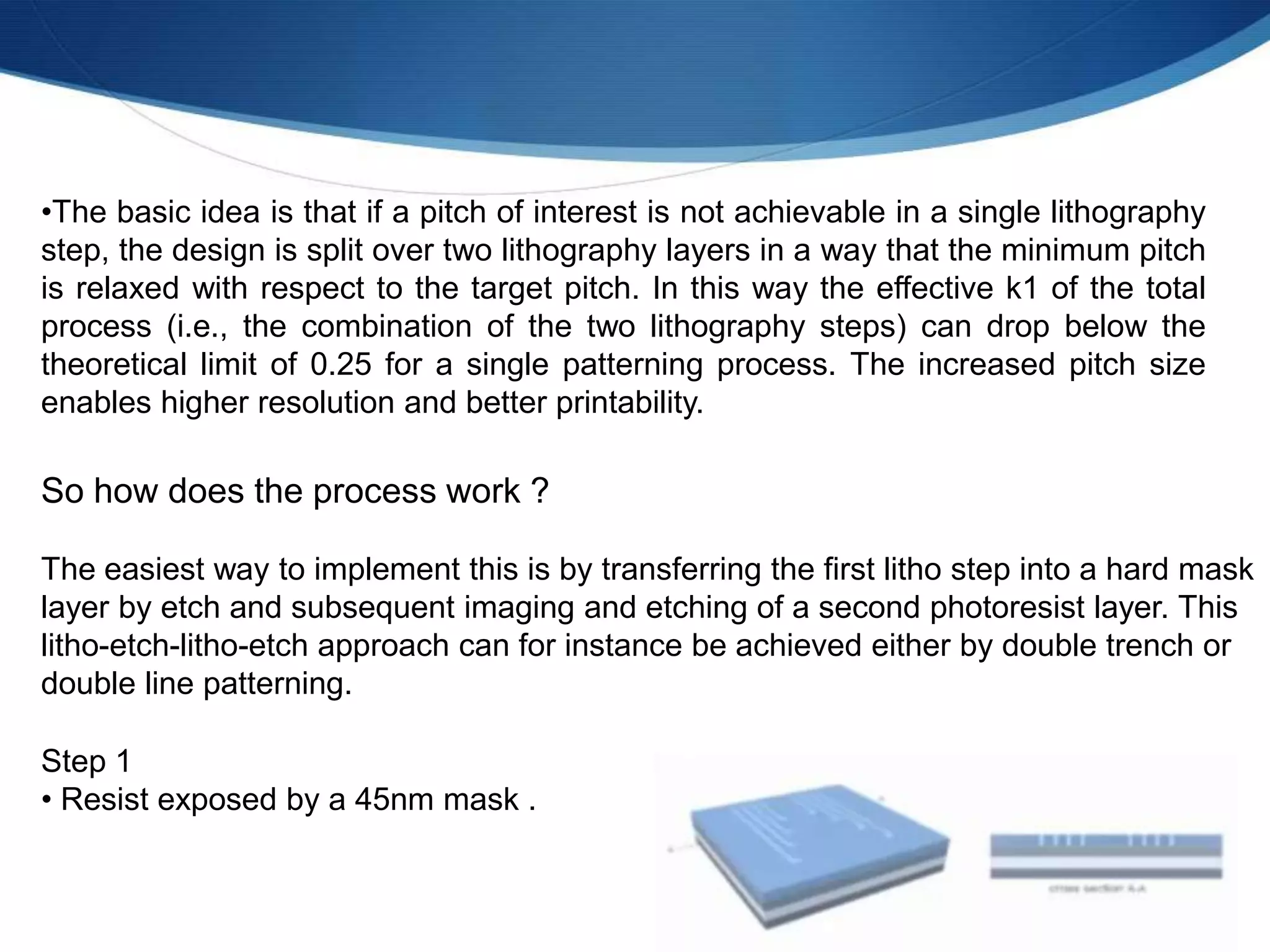
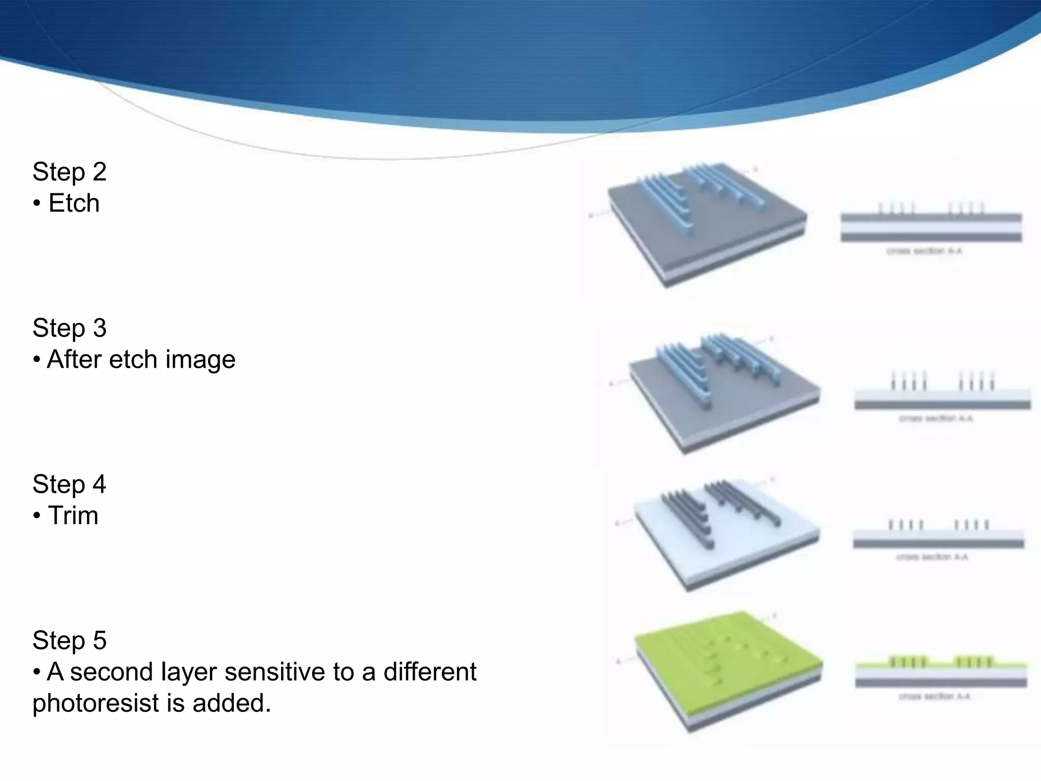


The document discusses double patterning lithography, a technique used to improve the resolution and minimize feature sizes in optical microlithography for semiconductor manufacturing at the 32nm half pitch node and beyond. It highlights how multiple patterning can effectively reduce the k1 coefficient below the theoretical limit of 0.25, enabling a higher pitch size and better printability. The process involves splitting designs over two lithography steps, showcasing the litho-etch-litho-etch approach to achieve smaller features safely and efficiently.