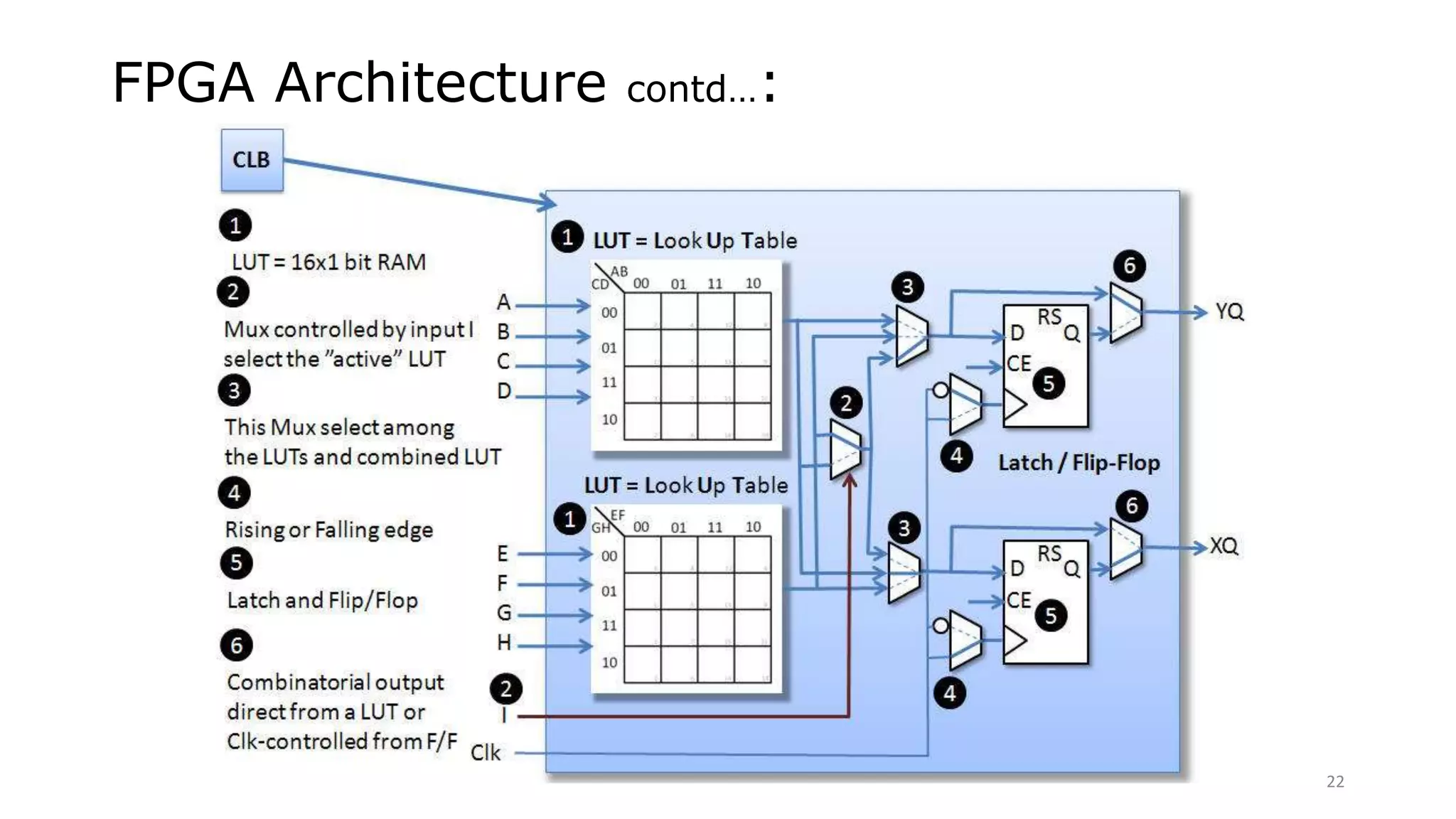
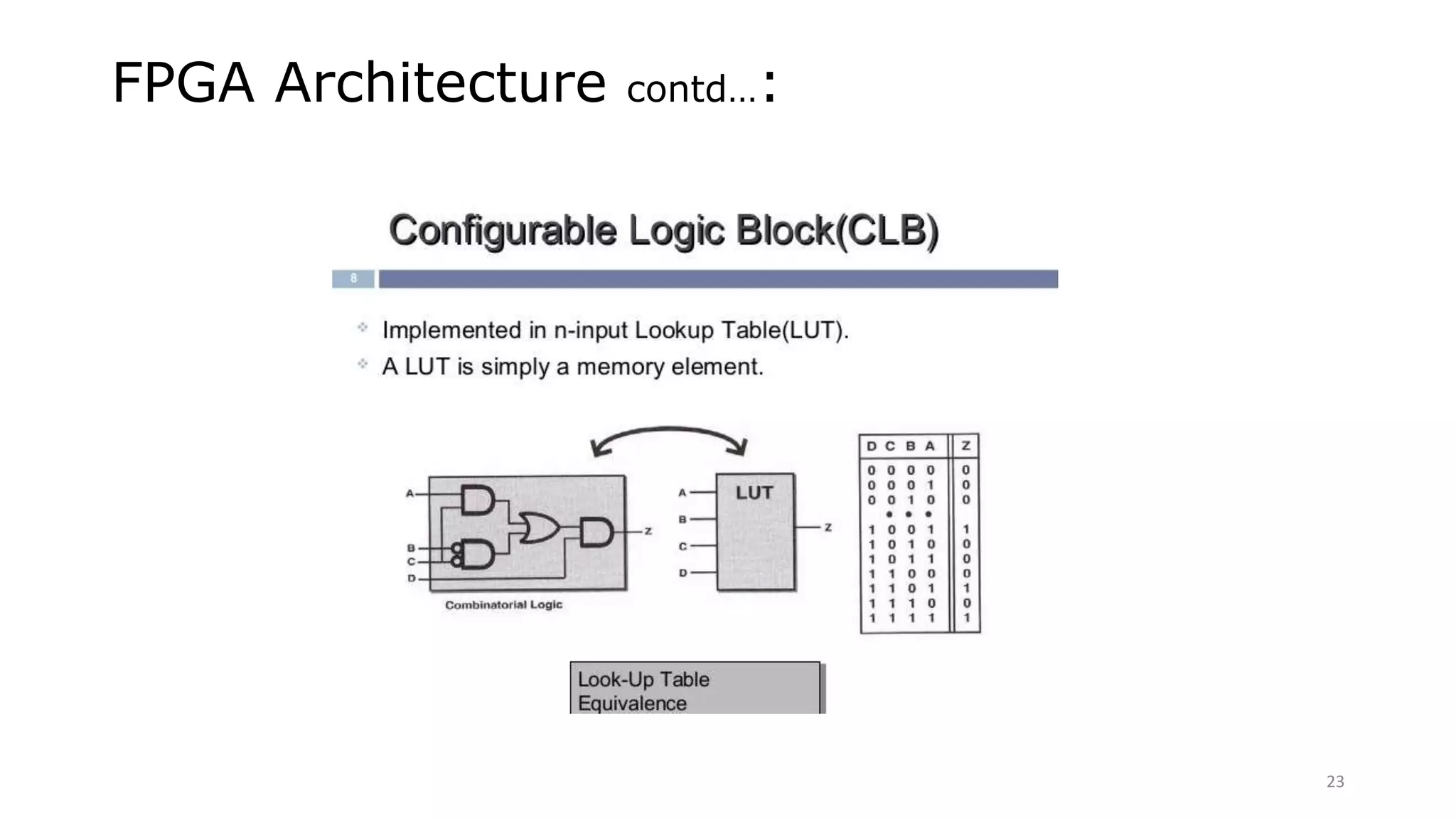
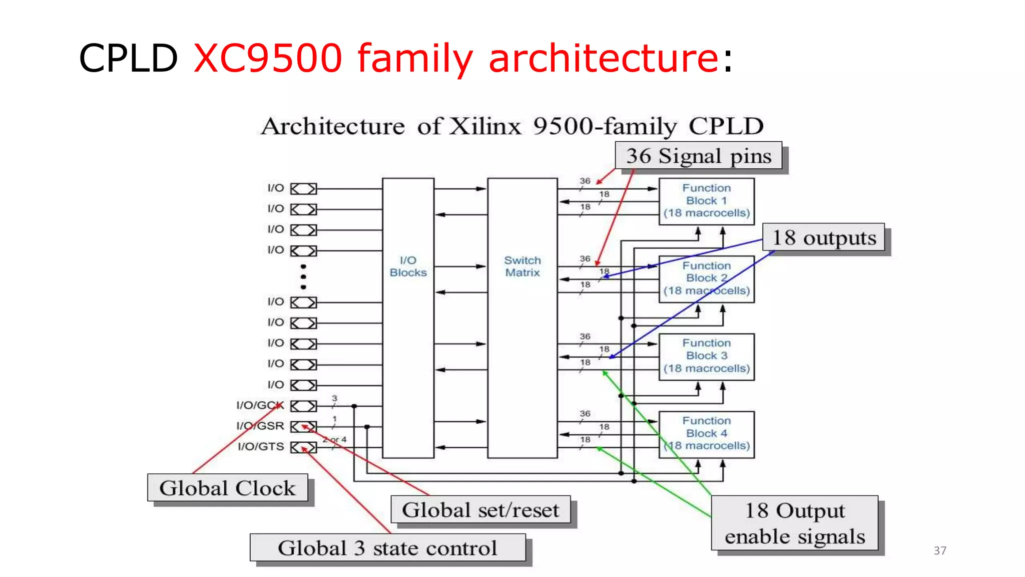
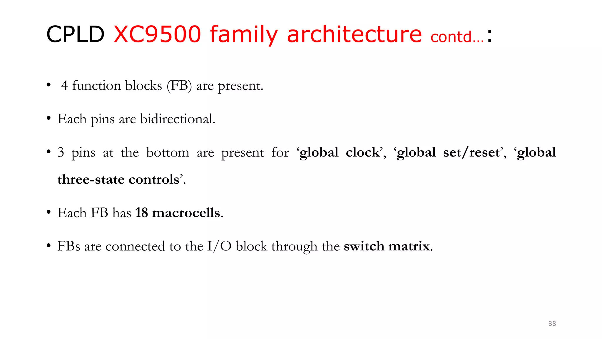
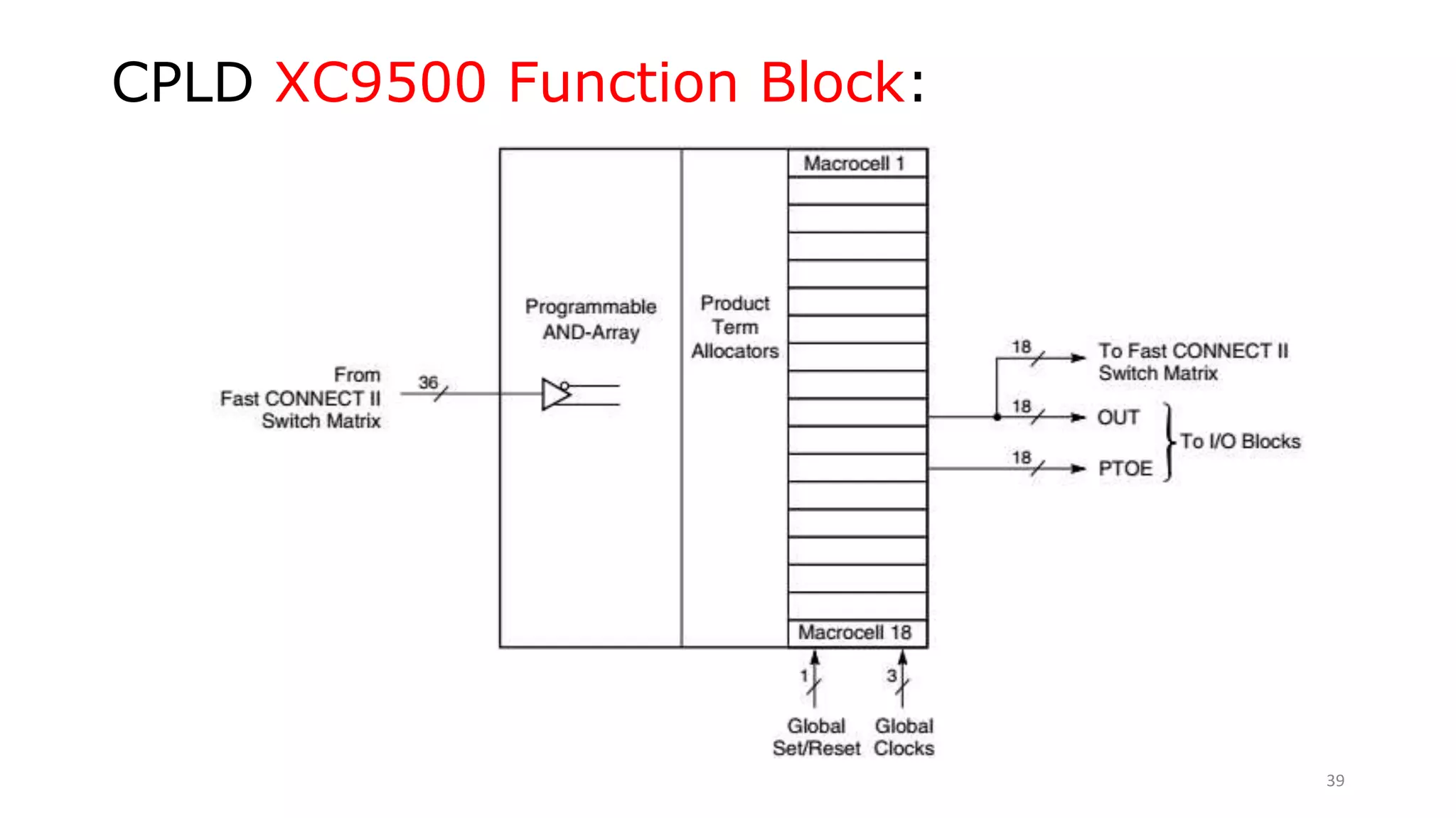
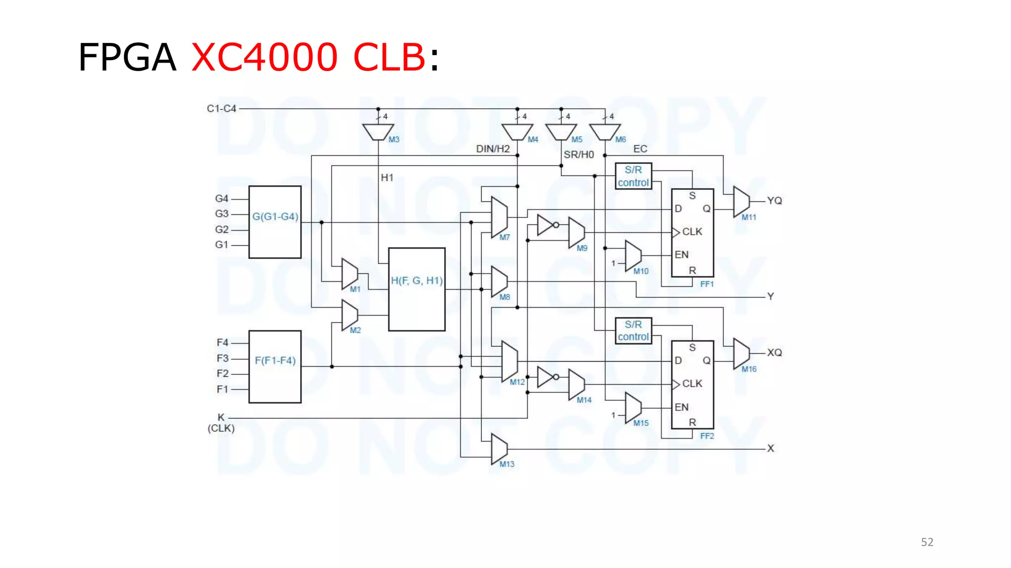
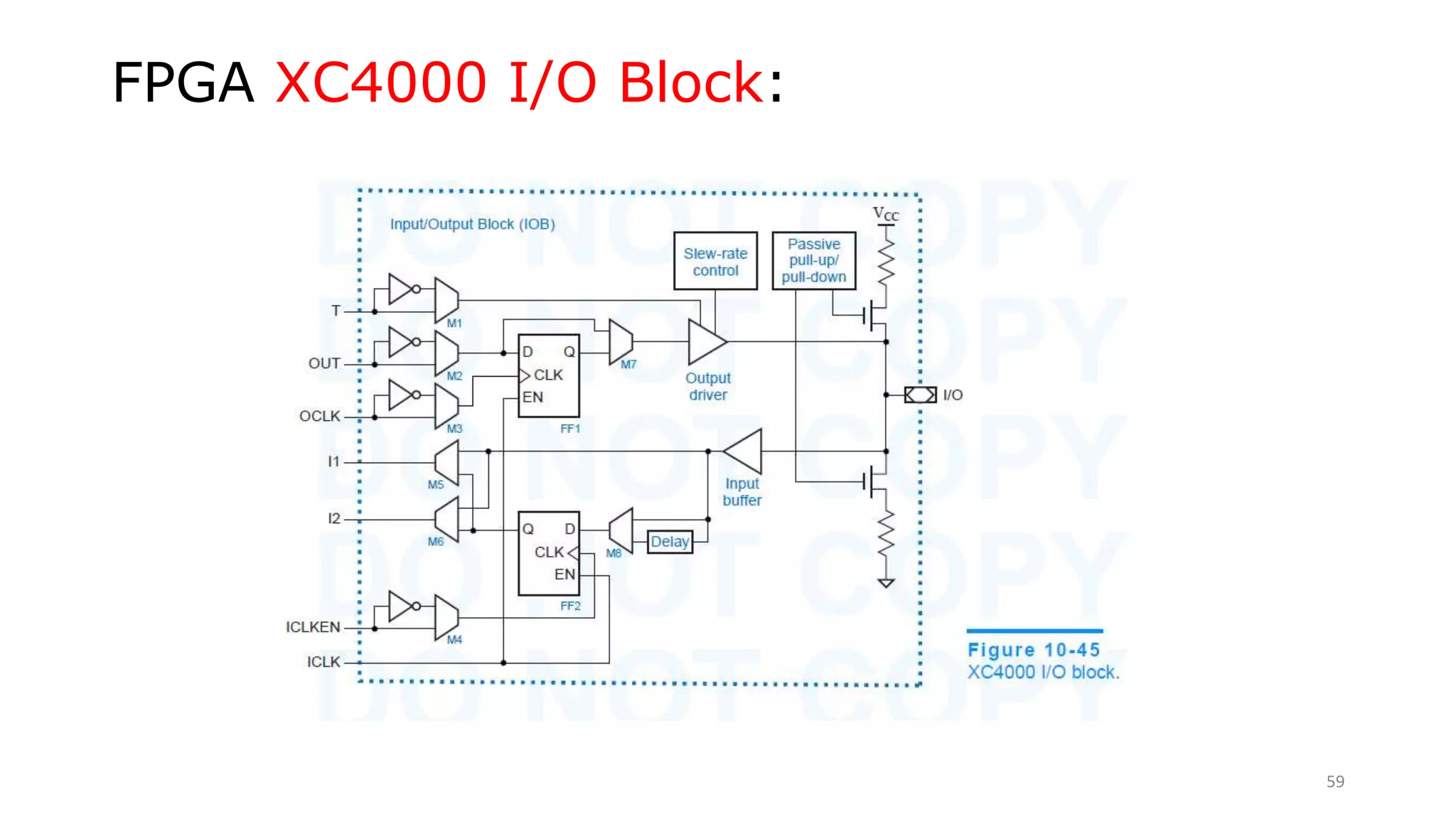
CPLD and FPGA(Refer: Digital Design - John F Wakerley {pages 898 – 916})
- Agi Joseph George,
AP / ECE / AJCE
1
Introduction:
• In the world of digital electronic systems, there are 3 basic kinds of devices:
• Memory, microprocessor, logic devices
• Memory devices store random information such as the contents of a spreadsheet or
database.
• Microprocessors execute software instructions to perform a wide variety of tasks
such as running a word processing Program or video game.
• Logic devices provide specific functions, including
• device-to-device interfacing,
• data communication,
• signal processing,
• data display,
• timing and control operations, and
• almost every other function a system must perform.
2
Logic Devices:
• A logic device is one which can perform any logic function
• Logic devices are broadly classified in to two categories:
• Fixed and
• Programmable.
• As the name suggests, the circuits in a fixed logic device are permanent, they
perform one function or set of functions – once manufactured, they cannot be
changed.
• On the other hand, programmable devices are standard and offers a wide range of
logic features and voltage characteristics - and these devices can be changed at any
time to perform various logic functions.
3
Programmable Logic Devices (PLDs):
• A programmable logic device is an integrated circuit with internal logic gates and
interconnects.
• These gates can be connected to obtain the required logic Configuration.
• The term Programmable means changing either hardware or software configuration
of an internal logic and interconnects.
• Of course the configuration of the internal logic is done by the user.
• PROM,EPROM,PAL,GAL etc.. are few examples of programmable logic devices.
4
Programmable Logic Devices contd…:
• A PLD is a general purpose chip for implementing logic circuitry.
• It contains a collection of logic circuit elements that can be customized in different
ways.
• A PLD can be viewed as a black box that contains logic gates and programmable
switches .
• These devices allow the end user to specify the logical operation of the device
through a process called “programming”
5
Types of PLDs:
• Among the several types of commercial PLDs available, there are two important
types.
• PLA (Programmable logic array)
• PAL (Programmable array logic)
6
Programmable logic array:
• The PLA was developed in the middle 1970s as the first non-memory programmable
logic device.
• It is used as programmable ‘AND’ array as well as programmable ‘OR’ array i.e., both
‘AND’ and ‘OR’ planes are programmable.
• Logic functions can be realized using SOP.
7
Programmable logic array contd…:
8
Programmable logic array contd…:
• Advantages:
• The architecture of PLA is more flexible.
• Frequently used in state machine design.
• Disadvantages:
• Although the PLA is more flexible it has not been widely accepted by engineers.
• Due to programmable ‘AND’ and ‘OR’ planes, more number of programmable switches are
required, which reduce the speed performance of the circuits implemented in PLAs.
9
Programmable Array logic (PAL):
• The drawbacks in PLA has led to the development of similar device in which the
‘AND’ plane is programmable, but ‘OR’ plane is fixed.
• Such a chip is known as a programmable array logic (PAL).
10
Programmable Array logic (PAL) contd…:
11
Programmable Array logic (PAL) contd…:
• Advantages:
• Frequently used in practical applications.
• Less expensive and offer better performance than PLA.
• Disadvantages:
• ROM guaranteed to implement any M functions of N inputs. PAL may have too few inputs to
the OR gates.
12
CPLDs & FPGAs:
• To retain the advantages and to overcome the disadvantages of PLAs and PALs the
newly introduced devices are known as CPLDs and FPGAs
• WHAT DO THEY DO?:
• These are reprogrammable logic devices .
• Designers use software to develop any digital circuit they like and the program the chip to
perform the function.
• They are very fast – much faster than a microcontroller.
13
CPLDs:
• Instead of relying on a programming unit to configure a chip , it is advantageous to
be able to perform the programming while the chip is still attached to its circuit
board. This method of programming is known as “In-System programming”
(ISP).
• It is not usually provided for PLAs (or) PALs , but it is available for the more
sophisticated chips known as “Complex programmable logic device”.
• “A Complex programmable logic device is a device that contain multiple
combination of PLAs and PALs”
14
CPLDs contd…:
15
Field programmable logic devices (FPGAs):
• Field programmable gate arrays (FPGAs) arrived in 1984 as an alternative to
programmable logic devices (PLDs) and ASICs.
• As their name implies ,FPGAs offer the significant benefit of being readily
programmable.
• FPGAs fill a gap between discrete logic and the smaller PLDs on the low end of the
complexity scale and costly custom ASICs on the high end.
16
FPGAs contd…:
• Just a few years ago, the largest FPGA was measured in tens of thousands of system
gates and operated at 40MHz.
• Older FPGAs often cost more than $150 for the most advanced parts at the time.
• Today, however, FPGAs offer millions of gates of logic capacity, operate at
300MHz, can cost less than $10, and offer integrated functions like processors and
memory
• FPGAs offer all of the features needed to implement most complex designs.
17
FPGAs contd…:
• “A Field Programmable Gate Array (FPGA) is a programmable logic device that
supports implementation of relatively large logic circuits.”
• As the name suggests, Field Programmable Gate Arrays the standard logic
elements are available for the designer.
• He has only to interconnect these elements to achieve the desired functional
performance.
18
FPGA Architecture:
• The architecture of FPGA is very simple than other programmable devices.
• The basic elements of an Field Programmable Gate Array are:
• Configurable logic blocks(CLBs)
• Configurable input output blocks(IOBs)
• Two layer metal network of vertical and horizontal lines for interconnecting the CLBS and
FPGAs (programmable interconnect)
19
FPGA Architecture:
20
FPGA Architecture contd…:
• CONFIGURABLE LOGIC BLOCK:
• Basic repeating logic resource on an FPGA.
• The components in CLBs execute complex logic functions, implement memory functions,
and synchronize code on the FPGA.
• CLBs contain smaller components, including flip-flops, look-up tables, and multiplexers.
• Flip-flop - Each flip-flop in a CLB is a binary shift register.
• Look-up Table (LUT) - A collection of gates hardwired on the FPGA. A LUT stores a predefined list
of outputs for every combination of inputs.
• Multiplexer—A circuit that selects between two or more inputs and then returns the selected input.
21
FPGA Architecture contd…:
22
FPGA Architecture contd…:
23
FPGA Architecture contd…:
• CONFIGURABLE I/O LOGIC BLOCK:
• Used to interface FPGA with external components.
• Is an arrangement of transistors for configurable I/O drivers.
24
FPGA Architecture contd…:
• CONFIGURABLE I/O LOGIC BLOCK
25
FPGA Architecture contd…:
• PROGRAMMABLE INTERCONNECTS:
• These are unprogrammed interconnection resources on the chip which have
channelled routing with fuse links.
• Provides the routing path used to connect the inputs and outputs of the IOBs and
CLBs into the logic network.
• Programmable highly interconnect matrix is available. In this case the design is that
of the interconnections and communications only.
26
FPGA Architecture contd…:
27
FPGA Advantages:
• Design cycle is significantly reduced. A user can program an FPGA design in a few minutes or
seconds rather than weeks or months required for mask programmed parts.
• High gate density i.e., it offers large gate counts. Compared with PLDs they are less dense.
• No custom masks tooling is required saving thousands of dollars(Low cost).
• Low risk and highly flexible.
• Reprogram ability for some FPGAs(design can be altered easily).
• Can replace currently used SSI and MSI chips.
• Suitable for prototyping.
28
FPGA Limitations:
• Speed is comparatively less.
• The circuit delay depends on the performance of the design implementation tools.
• The mapping of the logic design into FPGA architecture requires sophisticated
design implementation (CAD)tools than PLDs.
29
FPGA Vendors:
• Xilinx : Founded by Ross Freeman, original inventor of FPGAs in 1984.
• Sparten II,IIE,
• Sparten III,
• Virtex
• Altera:
• Altera cyclone II FPGA
• Actel
30
FPGA Applications:
• Low-cost customizable digital circuitry
• Can be used to make any type of digital circuit.
• High-performance computing performance
• Complex algorithms are off-loaded to an FPGA coprocessor
• Evolvable hardware
• Hardware can change its own circuitry.
• Neural Networks.
• Digital Signal Processing
• Reconfigurable DSP hardware
31
Xilinx CPLD Family
- XC9500
32
CPLD intro:
• Is a PLD with complexity between PALs and FPGA.
• And architectural features of both.
• Main block is a macrocell.
• Macrocell contains logic implemented in disjunctive normal form (SOP) and more
specialized operations.
• CPLDs are mainly meant for interfacing rather than heavy computation for
which FPGA is used.
33
CPLD XC9500 features:
• High-performance - 5 ns pin-to-pin logic delays on all pins.
• Large density range - 36 to 288 macrocells with 800 to 6,400 usable gates.
• 5V in-system programmable.
• Enhanced pin-locking architecture
• Called a ‘36V18’. That is, each PLD has 36 inputs and 18 macrocells.
• Not all macrocells are used for output. Some are used internally. They are called buried
macrocells.
• Same CPLD is available at different pin versions.
34
CPLD XC9500 device family:
35
CPLD XC9500 device family I/O pins:
36
CPLD XC9500 family architecture:
37
CPLD XC9500 family architecture contd…:
• 4 function blocks (FB) are present.
• Each pins are bidirectional.
• 3 pins at the bottom are present for ‘global clock’, ‘global set/reset’, ‘global
three-state controls’.
• Each FB has 18 macrocells.
• FBs are connected to the I/O block through the switch matrix.
38
CPLD XC9500 Function Block:
39
CPLD XC9500 Function Block contd…:
• The programmable AND array has 90 product terms.
• There are product term allocators that allow the unused product terms to be used
by other macrocells.
• PTOE – product term Output Enable
40
CPLD XC9500 product term allocator:
41
CPLD XC9500 product term allocator contd…:
• S1 – S8 are programmable steering elements.
• Connect their inputs to one of their 2 or 3 outputs.
• M1 – M5 are trapezoidal boxes.
• Are programmable MUX. Connect one of their 2 or 4 inputs to their output.
• 5 AND gates with the macrocell.
• Each connected to a signal steering box whose top output connects the product term to the
macrocell’s main OR gate G4. i.e., only 5 product terms per macrocell.
42
CPLD XC9500 product term allocator contd…:
• G4 has another input from G3 that receives product terms from the upper and lower
macrocells.
• Unused product terms are steered through S1 – S5 to be combined in an OR gate
G1 which is steered to macrocells above or below by S8.
• Can be combined with product terms above or below through S6, S7 and G2. they
are ‘daisy chained’.
• 90 product terms per FB.
43
CPLD XC9500 product term allocator contd…:
• Middle choice for each steering box S1 – S5 is to use the product term for a special
function.
• E.g.: flipflop clock, set or reset, XOR control or output enable.
• G4 forms an SOP expression and feeds to XOR gate G5. whose other input is M1.
• FF1 can be programmed to behave as DFF or TFF.
• M4 selects the flip-flop’s clock: from the 3 global clock or the product term.
• FF1 also has asynchronous set and reset inputs controlled by M2 and M5.
• M3 selects the FF1 output or the G5 output.
44
CPLD XC9500 I/O Block:
45
CPLD XC9500 I/O Block contd…:
• 7 choices for the 3 state buffer.
• Always on
• Always off
• Controlled by the PTOE
• Controlled by any of the 4 global output variables
• IOB provides analog controls in addition to logic ones.
• Slew-rate control
• Pull-up resistor
• User-programmable ground.
46
CPLD switch matrix(XC95108):
47
CPLD switch matrix(XC95108) contd…:
• Has 108 macrocell outputs and 108 external inputs.
• Total of 216 signals to be connected as input to the switch matrix.
• XC95108 has 6 FBs, each having 36 inputs, i.e., 216 inputs.
• Connecting the inputs 0 – 35 to the same Fb is difficult.
• As SM input 0 is connected to FB input 0, other inputs to the same FB are blocked.
• But we only need every input to be connectable to some input of the FB.
48
Xilinx FPGA Family
- XC4000
49
FPGA XC4000 Features:
• Flexible function generators.
• On-chip ultra fast RAM
• Abundant flip-flops.
• Hierarchy of interconnect lines
• Flexible array architecture.
• Backward compatible with XC4000 devices.
• Program verification – Read back.
• Low power segmented routing architecture.
• 2 flipflops per CLB and I/O.
50
FPGA XC4000 Family:
51
FPGA XC4000 CLB:
52
FPGA XC4000 CLB contd…:
• F, G and H are the most important logical function generators of the CLB.
• F and G perform any combinational logic function on their 4 inputs.
• H performs on its 3 inputs.
• Outputs of F and G and the additional CLB inputs are inputs to H by M1 - M3.
• With appropriate programming of M7 – M8 , M12 – M13, the outputs of the
function generators can be directed to the CLB outputs, X and Y or to the FF1 and
FF2.
53
FPGA XC4000 CLB contd…:
• FF1 and FF2 has common clock input, K, selected by the M9 and M14.
• They also make use of the Enable Clock signal, EC through M10 and M15.
• EC, and other internal signals, DIN/H2, H1, SR/H0 are selected from the C1 – C4
by M3 – M6.
• If no FF used in the CLB, then XQ or YQ can be selected to ‘bypass’ output from
the CLB input M4 or M6.
• S/R control determines whether the FF is set or reset.
54
FPGA XC4000 CLB Working:
• 4-input logic function is described by its truth table.
• The truth table is saved in a 16 word by 1-bit wide memory.
• The F and G are used as 16 x 1 SRAM and H is a 8 x 1 SRAM.
• F, G and H are loaded from an external ROM.
• The programmable MUXs are also controlled by the SRAM.
• The programming is done for all the CLBs in the FPGA.
55
FPGA XC4000 CLB Working contd…:
• Different modes of configuration:
• Two 16X1 SRAM – F and G are used as SRAMs with independent addresses and write-data inputs.
• One 32X1 SRAM – 4 bits of F and G and a 5th address bit is applied to the H.
• Asynchronous / synchronous – on the clock, K or asynchronous latching behaviour.
• One 16X1 dual port SRAM – two sets of address inputs used to independently read and write in
different locations of the same SRAM.
• F1-F4 and G1-G4 supply the address, H0-H2 provide data inputs and the write enable signal.
• Data outputs are provided by the F and G outputs.
56
FPGA XC4000 CLB Working contd…:
57
FPGA XC4000 CLB Working contd…:
58
FPGA XC4000 I/O Block:
59
FPGA XC4000 I/O Block contd…:
• Has more logic controls w.r.t to CPLD 9500.
• Input and output paths are selectable by M5 – M7.
• Other input signals come from the CLB array through the programmable
interconnect. They are OUT (output bit), OCLK (output clock), ICLKEN (input
clock enable) and T (tristate control).
• Like CPLD, there are analog signals like slew-rate control, pullup/down resistor.
60
FPGA XC4000 Programmable Interconnect:
61
FPGA XC4000 Programmable Interconnect contd…:
• Provides rich, symmetric connectivity,
• Wires with programmable connection.
• CLBs have 2 output wires going to the CLBs below and right of it.
• 2 set of input wires from the above and left CLBs.
• 4 wires for global clock.
• CLB connected to another using ‘Single’ wire have to go to a programmable switch.
• CLB can be connected to 2 CLBs using ‘Double’ wire.
• CLBs connected to ‘Long’ wires do not go through a programmable switch at all. They travel across
the row and column.
62

Cpld and fpga mod vi

  • 1.
    CPLD and FPGA(Refer:Digital Design - John F Wakerley {pages 898 – 916}) - Agi Joseph George, AP / ECE / AJCE 1
  • 2.
    Introduction: • In theworld of digital electronic systems, there are 3 basic kinds of devices: • Memory, microprocessor, logic devices • Memory devices store random information such as the contents of a spreadsheet or database. • Microprocessors execute software instructions to perform a wide variety of tasks such as running a word processing Program or video game. • Logic devices provide specific functions, including • device-to-device interfacing, • data communication, • signal processing, • data display, • timing and control operations, and • almost every other function a system must perform. 2
  • 3.
    Logic Devices: • Alogic device is one which can perform any logic function • Logic devices are broadly classified in to two categories: • Fixed and • Programmable. • As the name suggests, the circuits in a fixed logic device are permanent, they perform one function or set of functions – once manufactured, they cannot be changed. • On the other hand, programmable devices are standard and offers a wide range of logic features and voltage characteristics - and these devices can be changed at any time to perform various logic functions. 3
  • 4.
    Programmable Logic Devices(PLDs): • A programmable logic device is an integrated circuit with internal logic gates and interconnects. • These gates can be connected to obtain the required logic Configuration. • The term Programmable means changing either hardware or software configuration of an internal logic and interconnects. • Of course the configuration of the internal logic is done by the user. • PROM,EPROM,PAL,GAL etc.. are few examples of programmable logic devices. 4
  • 5.
    Programmable Logic Devicescontd…: • A PLD is a general purpose chip for implementing logic circuitry. • It contains a collection of logic circuit elements that can be customized in different ways. • A PLD can be viewed as a black box that contains logic gates and programmable switches . • These devices allow the end user to specify the logical operation of the device through a process called “programming” 5
  • 6.
    Types of PLDs: •Among the several types of commercial PLDs available, there are two important types. • PLA (Programmable logic array) • PAL (Programmable array logic) 6
  • 7.
    Programmable logic array: •The PLA was developed in the middle 1970s as the first non-memory programmable logic device. • It is used as programmable ‘AND’ array as well as programmable ‘OR’ array i.e., both ‘AND’ and ‘OR’ planes are programmable. • Logic functions can be realized using SOP. 7
  • 8.
  • 9.
    Programmable logic arraycontd…: • Advantages: • The architecture of PLA is more flexible. • Frequently used in state machine design. • Disadvantages: • Although the PLA is more flexible it has not been widely accepted by engineers. • Due to programmable ‘AND’ and ‘OR’ planes, more number of programmable switches are required, which reduce the speed performance of the circuits implemented in PLAs. 9
  • 10.
    Programmable Array logic(PAL): • The drawbacks in PLA has led to the development of similar device in which the ‘AND’ plane is programmable, but ‘OR’ plane is fixed. • Such a chip is known as a programmable array logic (PAL). 10
  • 11.
    Programmable Array logic(PAL) contd…: 11
  • 12.
    Programmable Array logic(PAL) contd…: • Advantages: • Frequently used in practical applications. • Less expensive and offer better performance than PLA. • Disadvantages: • ROM guaranteed to implement any M functions of N inputs. PAL may have too few inputs to the OR gates. 12
  • 13.
    CPLDs & FPGAs: •To retain the advantages and to overcome the disadvantages of PLAs and PALs the newly introduced devices are known as CPLDs and FPGAs • WHAT DO THEY DO?: • These are reprogrammable logic devices . • Designers use software to develop any digital circuit they like and the program the chip to perform the function. • They are very fast – much faster than a microcontroller. 13
  • 14.
    CPLDs: • Instead ofrelying on a programming unit to configure a chip , it is advantageous to be able to perform the programming while the chip is still attached to its circuit board. This method of programming is known as “In-System programming” (ISP). • It is not usually provided for PLAs (or) PALs , but it is available for the more sophisticated chips known as “Complex programmable logic device”. • “A Complex programmable logic device is a device that contain multiple combination of PLAs and PALs” 14
  • 15.
  • 16.
    Field programmable logicdevices (FPGAs): • Field programmable gate arrays (FPGAs) arrived in 1984 as an alternative to programmable logic devices (PLDs) and ASICs. • As their name implies ,FPGAs offer the significant benefit of being readily programmable. • FPGAs fill a gap between discrete logic and the smaller PLDs on the low end of the complexity scale and costly custom ASICs on the high end. 16
  • 17.
    FPGAs contd…: • Justa few years ago, the largest FPGA was measured in tens of thousands of system gates and operated at 40MHz. • Older FPGAs often cost more than $150 for the most advanced parts at the time. • Today, however, FPGAs offer millions of gates of logic capacity, operate at 300MHz, can cost less than $10, and offer integrated functions like processors and memory • FPGAs offer all of the features needed to implement most complex designs. 17
  • 18.
    FPGAs contd…: • “AField Programmable Gate Array (FPGA) is a programmable logic device that supports implementation of relatively large logic circuits.” • As the name suggests, Field Programmable Gate Arrays the standard logic elements are available for the designer. • He has only to interconnect these elements to achieve the desired functional performance. 18
  • 19.
    FPGA Architecture: • Thearchitecture of FPGA is very simple than other programmable devices. • The basic elements of an Field Programmable Gate Array are: • Configurable logic blocks(CLBs) • Configurable input output blocks(IOBs) • Two layer metal network of vertical and horizontal lines for interconnecting the CLBS and FPGAs (programmable interconnect) 19
  • 20.
  • 21.
    FPGA Architecture contd…: •CONFIGURABLE LOGIC BLOCK: • Basic repeating logic resource on an FPGA. • The components in CLBs execute complex logic functions, implement memory functions, and synchronize code on the FPGA. • CLBs contain smaller components, including flip-flops, look-up tables, and multiplexers. • Flip-flop - Each flip-flop in a CLB is a binary shift register. • Look-up Table (LUT) - A collection of gates hardwired on the FPGA. A LUT stores a predefined list of outputs for every combination of inputs. • Multiplexer—A circuit that selects between two or more inputs and then returns the selected input. 21
  • 22.
  • 23.
  • 24.
    FPGA Architecture contd…: •CONFIGURABLE I/O LOGIC BLOCK: • Used to interface FPGA with external components. • Is an arrangement of transistors for configurable I/O drivers. 24
  • 25.
    FPGA Architecture contd…: •CONFIGURABLE I/O LOGIC BLOCK 25
  • 26.
    FPGA Architecture contd…: •PROGRAMMABLE INTERCONNECTS: • These are unprogrammed interconnection resources on the chip which have channelled routing with fuse links. • Provides the routing path used to connect the inputs and outputs of the IOBs and CLBs into the logic network. • Programmable highly interconnect matrix is available. In this case the design is that of the interconnections and communications only. 26
  • 27.
  • 28.
    FPGA Advantages: • Designcycle is significantly reduced. A user can program an FPGA design in a few minutes or seconds rather than weeks or months required for mask programmed parts. • High gate density i.e., it offers large gate counts. Compared with PLDs they are less dense. • No custom masks tooling is required saving thousands of dollars(Low cost). • Low risk and highly flexible. • Reprogram ability for some FPGAs(design can be altered easily). • Can replace currently used SSI and MSI chips. • Suitable for prototyping. 28
  • 29.
    FPGA Limitations: • Speedis comparatively less. • The circuit delay depends on the performance of the design implementation tools. • The mapping of the logic design into FPGA architecture requires sophisticated design implementation (CAD)tools than PLDs. 29
  • 30.
    FPGA Vendors: • Xilinx: Founded by Ross Freeman, original inventor of FPGAs in 1984. • Sparten II,IIE, • Sparten III, • Virtex • Altera: • Altera cyclone II FPGA • Actel 30
  • 31.
    FPGA Applications: • Low-costcustomizable digital circuitry • Can be used to make any type of digital circuit. • High-performance computing performance • Complex algorithms are off-loaded to an FPGA coprocessor • Evolvable hardware • Hardware can change its own circuitry. • Neural Networks. • Digital Signal Processing • Reconfigurable DSP hardware 31
  • 32.
  • 33.
    CPLD intro: • Isa PLD with complexity between PALs and FPGA. • And architectural features of both. • Main block is a macrocell. • Macrocell contains logic implemented in disjunctive normal form (SOP) and more specialized operations. • CPLDs are mainly meant for interfacing rather than heavy computation for which FPGA is used. 33
  • 34.
    CPLD XC9500 features: •High-performance - 5 ns pin-to-pin logic delays on all pins. • Large density range - 36 to 288 macrocells with 800 to 6,400 usable gates. • 5V in-system programmable. • Enhanced pin-locking architecture • Called a ‘36V18’. That is, each PLD has 36 inputs and 18 macrocells. • Not all macrocells are used for output. Some are used internally. They are called buried macrocells. • Same CPLD is available at different pin versions. 34
  • 35.
  • 36.
    CPLD XC9500 devicefamily I/O pins: 36
  • 37.
    CPLD XC9500 familyarchitecture: 37
  • 38.
    CPLD XC9500 familyarchitecture contd…: • 4 function blocks (FB) are present. • Each pins are bidirectional. • 3 pins at the bottom are present for ‘global clock’, ‘global set/reset’, ‘global three-state controls’. • Each FB has 18 macrocells. • FBs are connected to the I/O block through the switch matrix. 38
  • 39.
  • 40.
    CPLD XC9500 FunctionBlock contd…: • The programmable AND array has 90 product terms. • There are product term allocators that allow the unused product terms to be used by other macrocells. • PTOE – product term Output Enable 40
  • 41.
    CPLD XC9500 productterm allocator: 41
  • 42.
    CPLD XC9500 productterm allocator contd…: • S1 – S8 are programmable steering elements. • Connect their inputs to one of their 2 or 3 outputs. • M1 – M5 are trapezoidal boxes. • Are programmable MUX. Connect one of their 2 or 4 inputs to their output. • 5 AND gates with the macrocell. • Each connected to a signal steering box whose top output connects the product term to the macrocell’s main OR gate G4. i.e., only 5 product terms per macrocell. 42
  • 43.
    CPLD XC9500 productterm allocator contd…: • G4 has another input from G3 that receives product terms from the upper and lower macrocells. • Unused product terms are steered through S1 – S5 to be combined in an OR gate G1 which is steered to macrocells above or below by S8. • Can be combined with product terms above or below through S6, S7 and G2. they are ‘daisy chained’. • 90 product terms per FB. 43
  • 44.
    CPLD XC9500 productterm allocator contd…: • Middle choice for each steering box S1 – S5 is to use the product term for a special function. • E.g.: flipflop clock, set or reset, XOR control or output enable. • G4 forms an SOP expression and feeds to XOR gate G5. whose other input is M1. • FF1 can be programmed to behave as DFF or TFF. • M4 selects the flip-flop’s clock: from the 3 global clock or the product term. • FF1 also has asynchronous set and reset inputs controlled by M2 and M5. • M3 selects the FF1 output or the G5 output. 44
  • 45.
    CPLD XC9500 I/OBlock: 45
  • 46.
    CPLD XC9500 I/OBlock contd…: • 7 choices for the 3 state buffer. • Always on • Always off • Controlled by the PTOE • Controlled by any of the 4 global output variables • IOB provides analog controls in addition to logic ones. • Slew-rate control • Pull-up resistor • User-programmable ground. 46
  • 47.
  • 48.
    CPLD switch matrix(XC95108)contd…: • Has 108 macrocell outputs and 108 external inputs. • Total of 216 signals to be connected as input to the switch matrix. • XC95108 has 6 FBs, each having 36 inputs, i.e., 216 inputs. • Connecting the inputs 0 – 35 to the same Fb is difficult. • As SM input 0 is connected to FB input 0, other inputs to the same FB are blocked. • But we only need every input to be connectable to some input of the FB. 48
  • 49.
  • 50.
    FPGA XC4000 Features: •Flexible function generators. • On-chip ultra fast RAM • Abundant flip-flops. • Hierarchy of interconnect lines • Flexible array architecture. • Backward compatible with XC4000 devices. • Program verification – Read back. • Low power segmented routing architecture. • 2 flipflops per CLB and I/O. 50
  • 51.
  • 52.
  • 53.
    FPGA XC4000 CLBcontd…: • F, G and H are the most important logical function generators of the CLB. • F and G perform any combinational logic function on their 4 inputs. • H performs on its 3 inputs. • Outputs of F and G and the additional CLB inputs are inputs to H by M1 - M3. • With appropriate programming of M7 – M8 , M12 – M13, the outputs of the function generators can be directed to the CLB outputs, X and Y or to the FF1 and FF2. 53
  • 54.
    FPGA XC4000 CLBcontd…: • FF1 and FF2 has common clock input, K, selected by the M9 and M14. • They also make use of the Enable Clock signal, EC through M10 and M15. • EC, and other internal signals, DIN/H2, H1, SR/H0 are selected from the C1 – C4 by M3 – M6. • If no FF used in the CLB, then XQ or YQ can be selected to ‘bypass’ output from the CLB input M4 or M6. • S/R control determines whether the FF is set or reset. 54
  • 55.
    FPGA XC4000 CLBWorking: • 4-input logic function is described by its truth table. • The truth table is saved in a 16 word by 1-bit wide memory. • The F and G are used as 16 x 1 SRAM and H is a 8 x 1 SRAM. • F, G and H are loaded from an external ROM. • The programmable MUXs are also controlled by the SRAM. • The programming is done for all the CLBs in the FPGA. 55
  • 56.
    FPGA XC4000 CLBWorking contd…: • Different modes of configuration: • Two 16X1 SRAM – F and G are used as SRAMs with independent addresses and write-data inputs. • One 32X1 SRAM – 4 bits of F and G and a 5th address bit is applied to the H. • Asynchronous / synchronous – on the clock, K or asynchronous latching behaviour. • One 16X1 dual port SRAM – two sets of address inputs used to independently read and write in different locations of the same SRAM. • F1-F4 and G1-G4 supply the address, H0-H2 provide data inputs and the write enable signal. • Data outputs are provided by the F and G outputs. 56
  • 57.
    FPGA XC4000 CLBWorking contd…: 57
  • 58.
    FPGA XC4000 CLBWorking contd…: 58
  • 59.
    FPGA XC4000 I/OBlock: 59
  • 60.
    FPGA XC4000 I/OBlock contd…: • Has more logic controls w.r.t to CPLD 9500. • Input and output paths are selectable by M5 – M7. • Other input signals come from the CLB array through the programmable interconnect. They are OUT (output bit), OCLK (output clock), ICLKEN (input clock enable) and T (tristate control). • Like CPLD, there are analog signals like slew-rate control, pullup/down resistor. 60
  • 61.
    FPGA XC4000 ProgrammableInterconnect: 61
  • 62.
    FPGA XC4000 ProgrammableInterconnect contd…: • Provides rich, symmetric connectivity, • Wires with programmable connection. • CLBs have 2 output wires going to the CLBs below and right of it. • 2 set of input wires from the above and left CLBs. • 4 wires for global clock. • CLB connected to another using ‘Single’ wire have to go to a programmable switch. • CLB can be connected to 2 CLBs using ‘Double’ wire. • CLBs connected to ‘Long’ wires do not go through a programmable switch at all. They travel across the row and column. 62